|
If this message is not displayed correctly, please click here.
|
September 2026 | Trade Fair News
|
|
SEMICON® TAIWAN
Leading with Collaboration. Innovating with the World.
|
|
Dear Visitor,
SEMICON Taiwan, the most influential semiconductor event in Taiwan, continues to serve as a key platform connecting the global semiconductor ecosystem. Building on three decades of growth, the exhibition reaches a record scale this year, bringing together 1,300 exhibitors across 4,300 booths and hosting more than 20 international forums. Under the theme “Transform Tomorrow,” SEMICON Taiwan 2026 will bring together global semiconductor leaders and leading companies to explore the industry’s next decade. The event will spotlight 15 key industry topics, including advanced manufacturing, quantum technology, sustainability, and semiconductor cybersecurity, highlighting the power of ecosystem collaboration in shaping the future of semiconductors.
As ties between Taiwan and Germany continue to strengthen, the German Pavilion once again brings together leading German companies to showcase their expertise and innovative solutions for the semiconductor industry. From semiconductor manufacturing and materials to testing, automation, and other advanced technologies, our exhibitors represent the strength and diversity of Germany’s semiconductor ecosystem and its contribution to the global supply chain.
In this special edition newsletter, you will find introductions to all exhibitors at the German Pavilion, including their company profiles and an overview of the products, technologies, and services they will present at SEMICON Taiwan 2026. We warmly invite you to visit the German Pavilion, meet our exhibitors, and explore new opportunities for cooperation.
Best regards,
Trade Fair Team
DEinternational Taiwan Ltd.
Service Unit of the German Trade Office Taipei |
German Pavilion Events
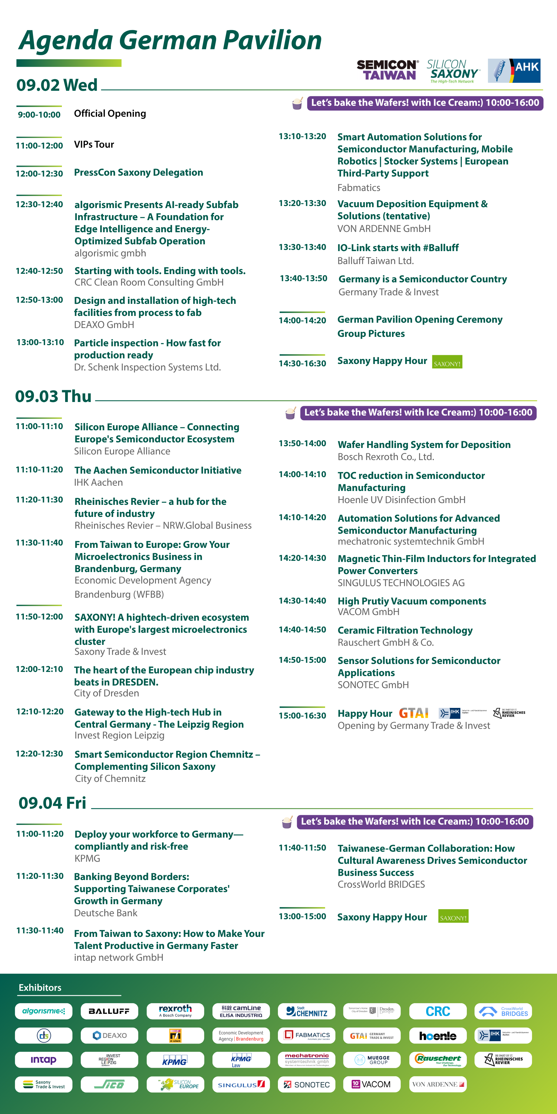
|
|
German Pavilion Exhibitors (in Alphabetical Order)
|
|
|
Please click the company name to get the information
|
|
Innovation in Subfab Sustainability:
Demand-Optimized Operations and Data Analytics for Significant CO2 Reduction in Semiconductor Manufacturing
algorismic is a German industrial IoT software company specializing in subfab automation and emission reduction for the semiconductor industry. Powered by real-time equipment data, its software solutions enable semiconductor fabs to monitor and control facility equipment such as abatement systems (scrubbers) and vacuum pumps. As a result, fabs can positively influence media consumption and reduce the environmental footprint of semiconductor manufacturing, cutting utility costs and CO2 emissions.
With a strong track record of successful deployments since 2023, the modular software delivers measurable efficiency gains alongside actionable visualizations. Engineered for comprehensive interoperability, the solution integrates seamlessly into existing fab IT infrastructures as well as greenfield facilities.
Whether driving substantial energy savings or optimizing resource consumption, algorismic empowers its partners to turn real-world sustainability challenges into significant OPEX savings and meet Scope 1 & 2 emission targets.
Learn more about algorismic on www.algorismic.com
|
|
|
Products / Service Introduction
|
|
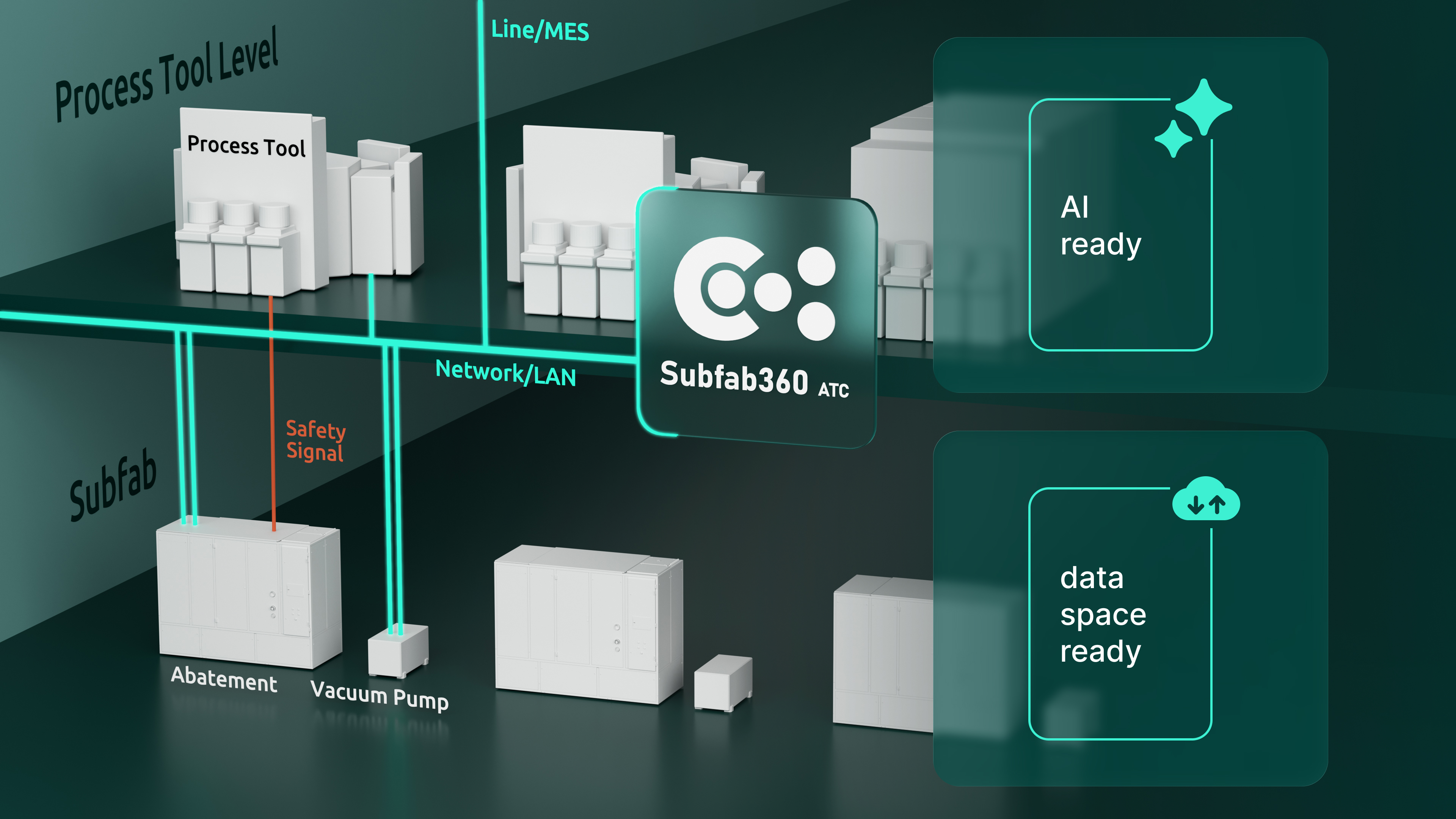
Subfab360 is algorismic’s software solution for running the subfab as efficiently and transparently as the cleanroom. It connects pumps, abatements, gas cabinets and process tools, turns their raw signals into a clear live picture and helps fabs cut energy, media use and emissions without changing existing equipment.
At its heart, Subfab360’s core continuously collects and organizes machine data and shows the status of all connected devices in one place. Engineers see where consumption rises, where alarms cluster and where standby times are possible – and can act before issues impact yield or uptime. Optional functional modules build directly on this shared data base:
- Subfab360 ATC (Active Tool Coupling) leverages the data foundation to enable abatement (scrubber) and vacuum pump control in real time delivering significant energy savings and reductions in CO₂ emissions, making it a true net zero roadmap enabler.
- Subfab360 Monitoring and data transfer modules open the subfab to MES, FDC and reporting tools, making equipment behaviour traceable and audit-ready.
- Subfab360 AI takes optimization further by applying edge AI to learn operational patterns and dynamically adapt parameters within defined safety limits.
Visualization and reporting modules then turn numbers into stories. Fleet dashboards show the health of the subfab, dashboard views reveal trends and reports translate savings into cost of ownership and payback times.
Because Subfab360 is manufacturer-independent and fits into existing fab IT landscapes, customers can start with one area, prove savings, and scale step by step – in brownfield sites as well as new fabs worldwide.
|
|
|
Balluff is a medium-sized company that has been family-run for four generations, was founded in Neuhausen auf den Fildern near Stuttgart and now has grown into a cosmopolitan, leading global player. We are a sensor and automation specialist with tradition and long-standing customer relationships, which at the same time is an important innovation partner for its customers.
Our company opened up to the international market at a very early stage. In the early 80s, Balluff began to continuously expand its production and sales network. Today, Balluff is no longer just at home in Neuhausen, but in Europe, Asia, North and South America and all other important markets - in 68 countries worldwide. This allows us to better understand and serve our customers and give them exactly what they need: high-quality sensor, identification and image processing solutions, including network technology and software for all their automation requirements. As a future-oriented company, we not only focus on the classic automation areas, but also respond to the continuously changing market needs of customers and a digital, networked world: As an empowerer, we enable our customers to achieve sustainable success in their digital transformation with IIoT-capable hardware, middleware and systems.
|
|
|
Products / Service Introduction
|
|
Application of Compact IO-Link Smart Sensors in Semiconductor Manufacturing
|
|
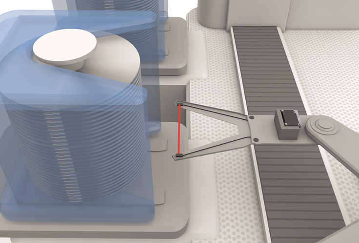
As semiconductor manufacturing continues to advance toward higher precision and miniaturization, the demand for compact, real-time, and intelligent sensing solutions is rapidly growing. IO-Link smart sensors offer plug-and-play connectivity, seamless integration, and continuous feedback, making them ideal for optimizing visibility and control in complex production environments. This session will highlight how IO-Link technology supports the semiconductor industry's goals of enhanced monitoring, predictive maintenance, and streamlined production through smart sensor integration.
Balluff solutions ensure extreme precision in every critical process step of semiconductor manufacturing.
- Wafer handling
- Wafer processing
- Carrier handling
- Vacuum applications
|
|
|
Real-Time Machine Insights with Balluff Condition Monitoring Toolkit
|
|
|
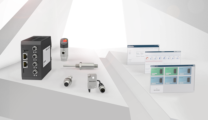
Unscheduled stoppages and faults in the production process can be avoided using the multi-functional condition monitoring sensors and integrated data pre-processing. Because these intelligent sensors provide you with condition information which you can use for automating costintensive manual inspections. Thiscondition data is also an important component of the IIoT for implementing smart and flexible manufacturing.
- Unified retrofit solution for machine and process monitoring
- Highly flexible through the connection of any four IO-Link sensors
- Easy and fast commissioning of the condition monitoring sensor
- Plug-and-play commissioning of the system and visualization of the data
- Autonomous system with data storage – independent of cloud and controller
- Remote monitoring through network integration via MQTT
- Customizable through docker support
- Comprehensive support from our application specialists
|
|
|
|
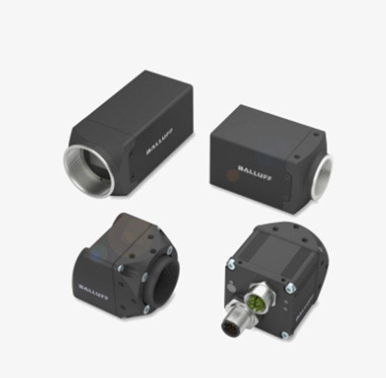
Balluff SWIR Cameras capture images in the short-wave infrared spectrum (900-1700nmnm), enabling machine vision systems to detect features that conventional visible-light cameras cannot see. SWIR imaging enables inspection through silicon and other semi-transparent materials, revealing features hidden from conventional visible-light cameras, packaging films, plastics, and other semi-transparent materials, making it ideal for semiconductor manufacturing and advanced industrial inspection.
Typical applications include wafer inspection, die alignment, edge crack detection, contamination detection, moisture Detection, Semiconductor package inspection, and inspection of bonded or encapsulated components. Combined with high-resolution imaging and GigE Vision connectivity, Balluff SWIR Cameras improve defect detection accuracy, process control, yield enhancement, and equipment reliability in semiconductor fabs and automated production lines.
|
|
|
|
As one of the world's leading suppliers of drive and control technologies, Bosch Rexroth ensures efficient, powerful, and safe movement in machines and systems of any size. The company bundles global application experience in the market segments of Mobile Applications, Industrial Applications & Engineering, and Factory Automation.
A wholly-owned subsidiary of the Bosch Group, the company was formed in 2001 through the merger of Mannesmann Rexroth AG and the Bosch Automation Technology business unit, with its technological roots dating back to 1795. Headquartered in Germany, Bosch Rexroth operates in over 80 countries, providing a global network of expertise and support.
For its customers, Bosch Rexroth develops tailored solutions that are safe, efficient, intelligent, and powerful. With its cross-technology portfolio—including hydraulics, electric drives and controls, and linear motion and assembly technology—the company is a reliable partner for machine manufacturers and end-users worldwide. By providing intelligent components, customized system solutions, and digital services, Bosch Rexroth is a key driver of digital transformation in manufacturing. We are actively shaping the "Factory of the Future," enabling seamless connectivity and sustainable production to help our customers enhance their competitiveness. WE MOVE. YOU WIN.
|
|
|
Products / Service Introduction
|
|
Wafer Pin Lift for Deposition Process
|
|
|
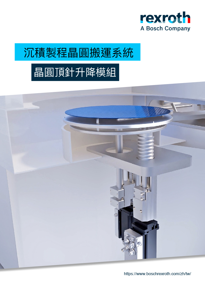
The Bosch Rexroth Wafer Pin Lift mechanism is specifically designed for semiconductor deposition processes, providing high-precision wafer lifting and positioning. It utilizes high-rigidity linear components, anultra-compact drive system, and high-response servo motors to achieve excellent positioning accuracy (±10-30 µm) and stable lifting control. The system is suitable for high vacuum and high-temperature environments (e.g.,PVD/CVD) and is manufactured with ultra-clean,low-outgassing materials compliant with ISOClass 5 cleanroom standards. It ensureslong-term reliability, meeting the stringentdemands for high precision and dependability inadvanced semiconductor manufacturing.
|
|
|
|
camLine has been recognized as a valued IT solution partner for high-tech manufacturing over the past 35 years. Industry automation systems are based on MES/MOM modules. Numerous implementations can be found in semiconductors, electronics, automotives, solar, batteries, medical devices, and renewable energies across Europe, North America, and APAC. In addition to service domains on quality assurance, process integrity, production logistics, OEE, monitoring and reporting, camLine’s solutions feature the orchestration of shop floor activities among different communication layers. As part of Elisa IndustrIQ, AI and machine learning (AI/ML) techniques are integrated in statistical methods to foster optimal engineering analysis and defect control.
|
|
|
Products / Service Introduction
|
|
LineWorks SPACE is camLine’s enterprise-grade advanced Statistical Process Control (SPC)solution tailored for semiconductor and high-techmanufacturing.
It real-time evaluates thousands of control chartsand massive data streams using 81 built-in SPC rules and trend analysis for early anomaly detection. Featuring instant equipment feedback,Troubleshooting Guides (TSG), automated control limit calculations, and interactive web-basedcharts, it helps multi-site facilities unify quality standards, boost yield, and achieve zero-defect manufacturing.
|
|
|
RACE™ Suite is camLine’s advanced MaterialControl System (MCS) and dispatching software package engineered for semiconductor andhigh-tech manufacturing.
It seamlessly bridges MES with AMHS hardware tooptimize real-time scheduling, dynamic routing,and automated dispatching for wafers andFOUPs. By actively eliminating material flow bottlenecks and preventing improper lot loading,RACE™ maximizes tool utilization and significantly reduces Work-in-Progress (WIP) waiting times.Highly scalable from single cells to fully automated mega-fabs, it serves as the intelligent software backbone driving smooth, automated shop-floor logistics.
|
|
|
iCADA Suite is camLine’s dedicated lifecycle management software engineered for high-value durables, reticles, andprobe cards in semiconductor manufacturing.
It provides end-to-end tracking, status control, and maintenance management for essential production toolingacross both front-end and back-end environments. By seamlessly integrating with MES and equipment, iCADA Suite monitors usage history, cleaning cycles, and degradation parameters in real time. It automates preventive maintenance scheduling, prevents incorrect tool mounting,and enforces strict inspection workflows. This optimizes asset utilization, extends tool longevity, and protects yields from defective or worn-out manufacturing durables.
|
|
|
City of Dresden - Economic Development Office
|
|
|
The City of Dresden’s Economic Development Office is your partner in Europe’s leading semiconductor region—Silicon Saxony. Dresden is home to global chip leaders such as TSMC and boasts a unique network of innovative high-tech companies, world-class universities and cutting-edge research institutes. A qualified talent pool, strategic location, advanced infrastructure, and strong focus on R&D make Dresden an ideal destination for semiconductor investments.
|
|
|
Products / Service Introduction
|
|
|
Business Services Dresden
|
|
|
The Business Services is the central information and advice center for investors and companies in Dresden.
Our office supports investors with comprehensive, free-of-charge services—from site selection, funding advice, and administrative guidance—delivered with industry expertise and direct access to talent and stakeholders within a thriving ecosystem.
|
|
CRC Clean Room Consulting GmbH
|
|
|
CRC Clean Room Consulting GmbH is a leading independent engineering consultancy specializing in the planning and design of high-tech production and research facilities. Headquartered in Freiburg, Germany, with over 40 years of experience, CRC is a global expert and trusted partner for semiconductor manufacturers worldwide.
With deep expertise in wafer fabrication, CRC has contributed to more than 750 semiconductor and wafer fab projects worldwide, including over 30 greenfield fabs and more than 1,000,000 sqm of cleanroom and production space.
CRC provides the full range of facility engineering services including:
- CSA
- Mechanical
- Cleanroom
- Process
- Electrical
- Automation / LS
- AMHS
- Equipment-Hook Up
- Tool Move in
A particular strength lies in delivering complex projects under the EPCM model, where CRC takes integrated responsibility for engineering, procurement, and construction management. Our designs follow a process-first approach: starting from tool layout and equipment requirements, we engineer cleanroom and infrastructure from the inside out to ensure optimal process flow, utility efficiency, and flexibility for future technology upgrades.
As a dedicated expert and trusted partner to the global semiconductor industry, CRC combines technical excellence, decades of fab experience, and a collaborative approach to turn highly complex challenges into world-class production environments.
|
|
|
Products / Service Introduction
|
|
Wafer Fab & Cleanroom Facility Engineering
|
|
|
In semiconductor manufacturing, the cleanroom environment determines yield, process stability, and scalability. CRC designs and engineers wafer fab environments to the highest international standards, utilizing process-driven and tool-first methodology, that systematically designs facilities from the inside out. The starting point for all planning decisions is based on the specific tools, processes, and production flows, from which integrated cleanroom, media, and utility concepts are developed.
CRC's expertise covers cleanroom design (ISO 1–9, dry rooms to –60 °C dew point), ultra-pure and process media systems, lab design, and full MEP/TGA engineering. The technical scope includes HVAC, power supply, life safety systems, gas and leak detection, and equipment hook-up. Through the close integration of all technical disciplines, CRC delivers robust, scalable fab concepts where processes, infrastructure, and the building structure form a functional unit, specifically designed to adapt to future technology nodes and evolving production requirements.
|
|
|
|
A core competency of CRC is the delivery of complex high-tech projects under the Engineering, Procurement and Construction Management (EPCM) model. In this role, CRC takes full integrated responsibility for planning, procurement, and execution, strictly ensuring schedule compliance, cost control, and premium quality across all project phases.
Semiconductor, wafer fab, and photonics projects in particular benefit from CRC's ability to combine deep technical expertise with professional project management. As a general planner, CRC assumes comprehensive contractual responsibility for all disciplines, including architecture, MEP, and process engineering. This provides clients with a single, experienced point of contact from the first concept to the final building handover. The goal is to achieve an overall optimum through synergies across all systems, establishing highly efficient and future-proof supply structures for semiconductor fabs and research facilities.
Through this approach, CRC minimizes interface risks, accelerates project timelines, and provides maximum planning reliability for high investment fab projects.
|
|
|
Facility Design & Architecture
|
|
|
CRC combines technical excellence with strong expertise in the architectural planning and realization of demanding industrial facilities.The goal is to deliver highly functional, technically optimized fab and cleanroom buildings that meet the complex production requirements of the semiconductor industry while balancing architectural, regulatory, and operational demands.
CRC's facility design strictly follows the inside-out principle, ensuring full alignment with the unique requirements of advanced semiconductor and wafer fab projects. Starting point is always the core processes, tools, cleanrooms, and MEP systems that define fab operations. On this solid foundation, CRC develops precise building structures that ensure long-term functionality, scalability, and operational reliability.
Critical factors such as spatial layouts, media routing, maintenance concepts, construction phasing, and permitting requirements are integrated into the building concept at a very early stage. The result consists of robust, scalable fab buildings that optimally support technological operations and secure the long-term commercial success of production sites.
|
|
|
|
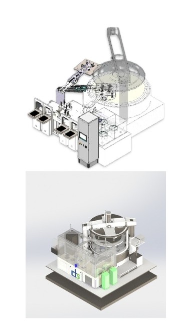
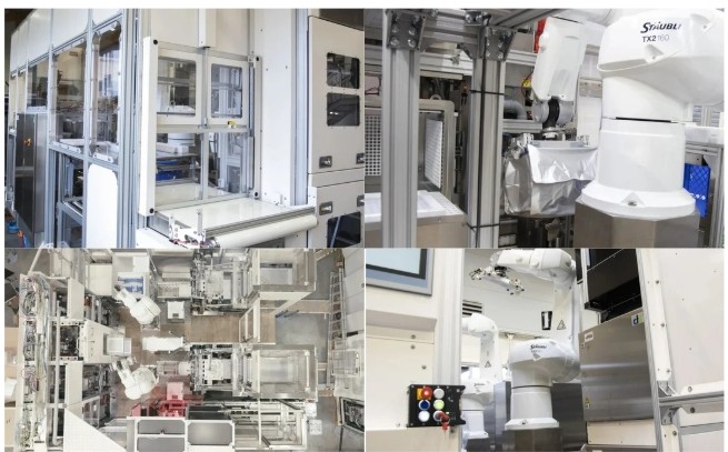
The cts Group automates industries across four business divisions: Process Automation, Manufacturing Automation, Industrial IT, and Energy Technology. The Manufacturing Automation division supports semiconductor manufacturers where every contact with a wafer is a risk to yield. cts plans and integratescleanroom-grade handling automation – from camera-based wafer handling in lapping and polishing processes through fully automated packaging of FOSBs – covering design, integration, and commissioning. Each solution is built around the customer's actual process, cleanliness class, and machine landscape, not the other way around. The result is a traceable, low-contact material flow that protects fragile carriers and contributes to stable, repeatable line yield.
|
|
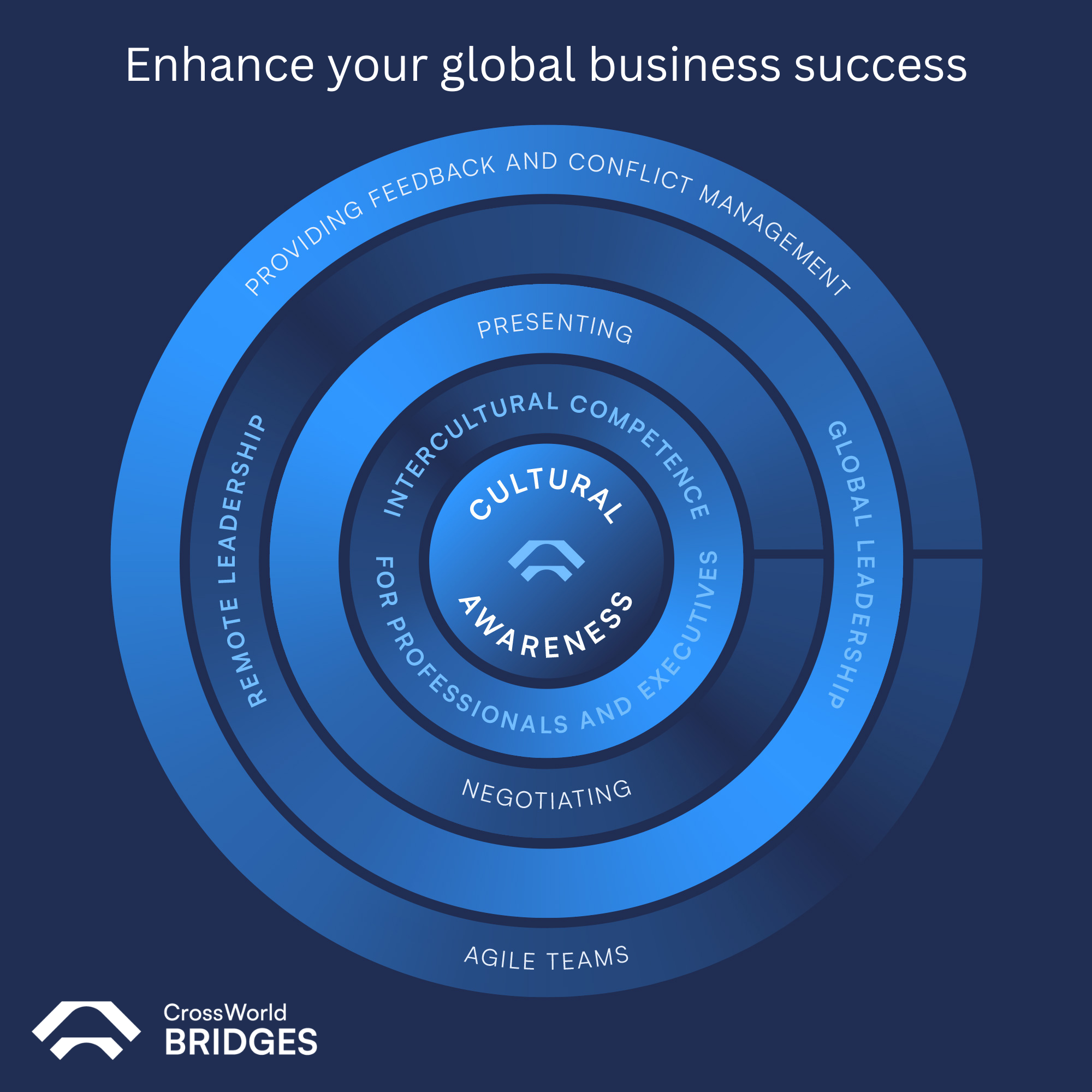
Intercultural Training and consulting services
|
|
|
CrossWorld BRIDGES provides intercultural training and consulting services for the semiconductor industry, with a strong focus on enabling effective collaboration between Taiwan, Germany, and global teams. In today’s highly complex and fast-moving semiconductor ecosystem, technical excellence alone is not sufficient to ensure successful projects. Misunderstandings in communication, differences in decision-making styles, and varying cultural expectations can significantly affect efficiency, delivery timelines, and trust between partners.
Our services help organizations bridge these gaps by building practical intercultural competence for engineers, managers, and international project teams. We support clients in improving communication clarity, reducing friction in cross-border collaboration, and strengthening long-term business relationships. By combining real-world international business experience with proven intercultural frameworks, we enable teams to work more effectively across cultural boundaries and organizational interfaces.
The result is smoother cooperation, faster alignment, fewer costly misunderstandings, and stronger global performance, transforming cultural diversity into a sustainable competitive advantage within the semiconductor industry worldwide.
|
|
|
|
Products / Service Introduction
|
|
Apollu: Wafer Handling in Lapping and Polishing
|
|
In lapping and polishing, surface quality and dimensionalaccuracy are defined at the micron level — and the handling step, not the process itself, is where most defects originate.Manual loading and unloading introduces scratches, edge damage, and particle contamination precisely where the wafer is most exposed.
Apollu addresses this through camera-based positioning: each wafer is optically detected and handled contactlessly,eliminating the operator-induced variability that conventional handling carries. The system processes wafer sizes from 150 to300 mm independent of the machine manufacturer, at a cycle time below 20 seconds, and operates within ISO-7 cleanroom conditions.
The relevant shift is conceptual. Handling stops being a manual interlude between process steps and becomes a controlled,repeatable part of the process chain — measurable,contamination-bounded, and decoupled from operator skill.Surface integrity is no longer something to protect after the fact, but a designed-in property of the handling step.
|
|
|
ABT: Automated FOSB Packaging
|
|
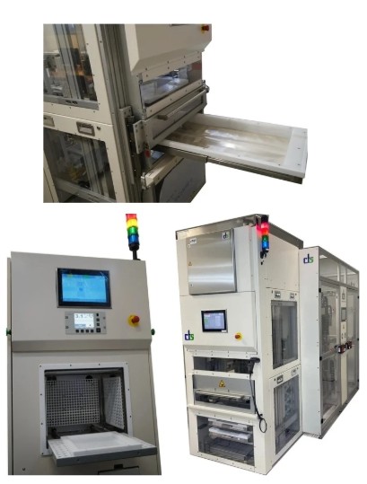
FOSB packaging is often treated as a logistics endpoint, but in traceability terms it is a critical control point. Two failure modes matter: a carrier-to-wafer mismatch breaks the data lineage, and a compromised seal exposes wafers duringtransport and storage. Both are difficult to detect downstream and expensive to trace back.
ABT automates the full sequence – identification, cross-slot verification, 100 % leak testing, and labeling – as a closed process. Code identification binds each FOSB to its correct wafer set, preserving lineage. Cross-slot checks and complete leak testing move quality control upstream, catching faults before transport rather than after. SECS/GEM compatibility connects the step to host systems, so packaging data is recorded rather than reconstructed.
The principle is that packaging belongs inside the traceability architecture, not adjacent to it. When identification,inspection, and documentation are automated together, the packaging step generates verifiable data instead of consuming it.
|
|
|
MBT: Semi-Automated Packaging
|
|
Full automation assumes volume and repetition. Prototype runs, qualification batches, and custom production invert that assumption: changeover frequency is high, quantities are low, and rigid automation becomes a constraint rather than an advantage.
MBT is built around a deliberate division of labor. Manual handling retains flexibility where product and process vary; automated core functions — including leak testing and carrier adjustment — preserve the quality standards that low volume cannot be allowed to compromise. The result is selective automation: human judgment where variation lives,machine consistency where the standard is fixed.
This reflects a broader point about fab automation. The question is not whether to automate, but which parts of aprocess genuinely benefit from it. For low-volume, high-mix environments, a semi-automated architecture is not a downgrade from full automation — it is the more accurate match to how the work actually behaves.
|
|
|
|
THE ENGINEERING COMPANY
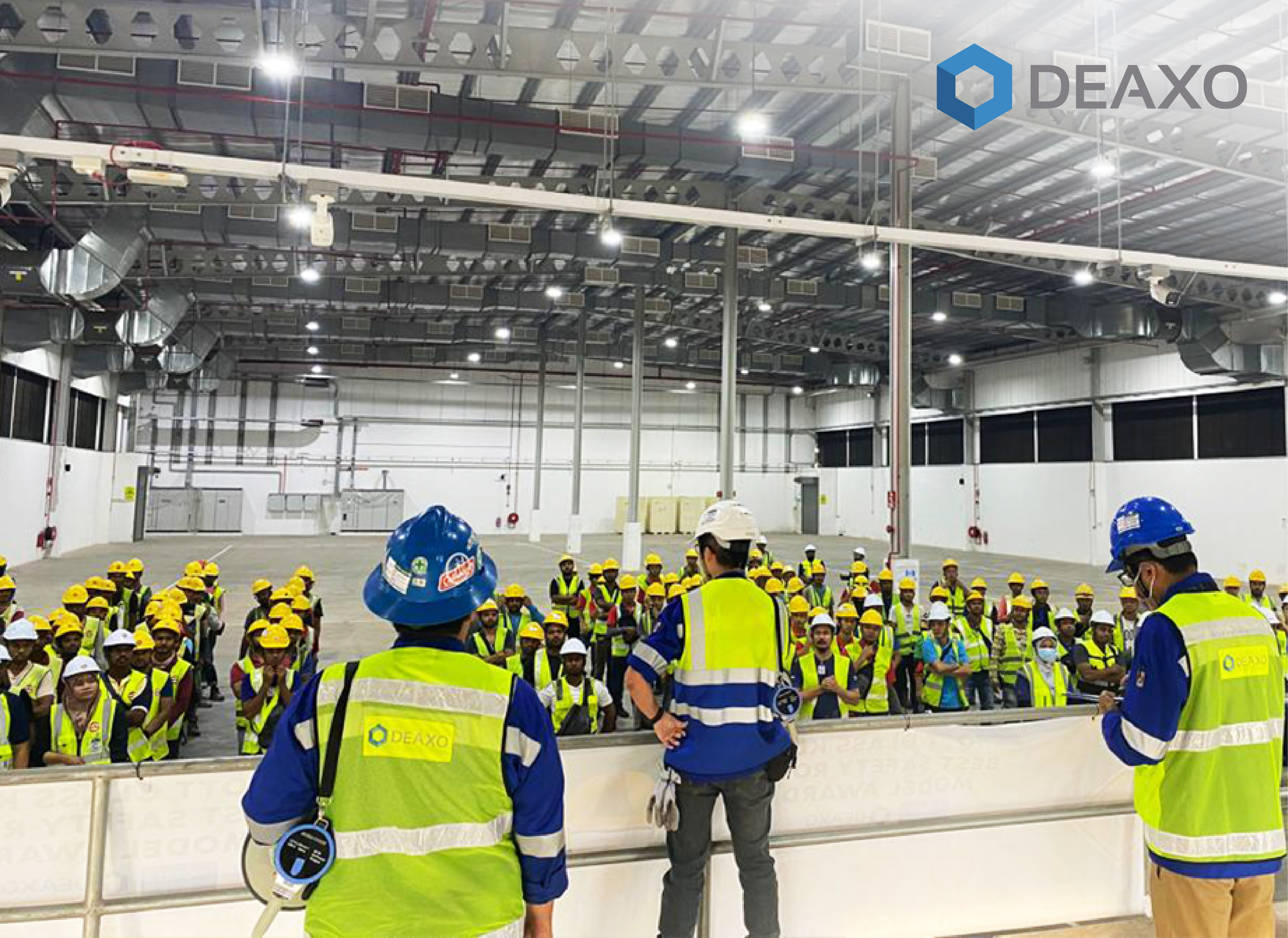
DEAXO is a specialized engineering company for high-tech projects with headquarter in Dresden, the heart of Silicon Saxony and one of Europe’s leading semiconductor hubs.
Our expertise lies in the design, engineering and realization of complex production environments,including semiconductor fabs, laboratories, cleanrooms and process facilities. We support clients throughout the entire project lifecycle - from feasibility studies and conceptual design to detailed engineering, construction management, commissioning and tool Hook-Up for both new fabs and upgrades of the existing ones.
We think of factories as systems. With decades of international industry experience, we bring together engineering excellence and an integrated approach that connects production processes, facility systems and operational requirements from the outset.
Our approach goes beyond technical design by considering the long-term performance and reliability of every facility. We take responsibility for managing complex projects with clarity and discipline,enabling our clients to benefit from greater cost efficiency and enhanced project control.
DEAXO collaborates with clients as an EPC, EPCM or PMC partner to create safe, reliable and production-ready facilities that enable technological progress.
|
|
|
Products / Service Introduction
|
|
|
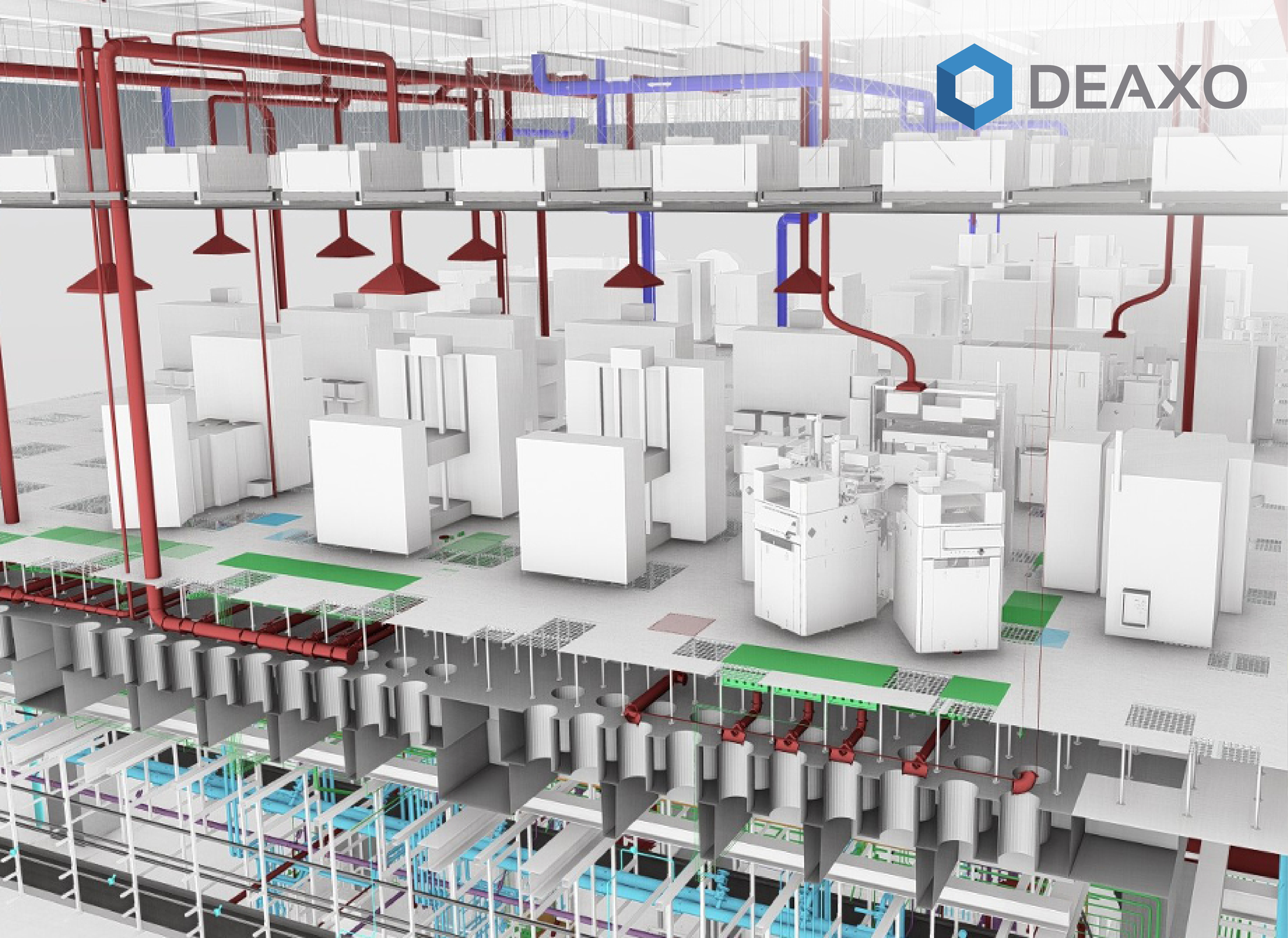
Our design approach is based on an operational perspective. By aligning process requirements,facility systems and operational needs from the earliest project stages, we create the foundation for efficient project delivery. This enables transparent decision-making, streamlined collaboration, and the flexibility to respond effectively to evolving project requirements. The use of advanced BIM technologies supports fast and reliable collaboration across all project teams.
Our scope of services covers design from process to fab, including the following work packages:
- Cleanroom
- Supply air
- Exhaust treatment
- Cooling & heating
- Special gases
- Chemicals & slurry
- Ultra-pure water
- Waste water treatment
- Electrical & controls
- Bulk gases
- Industrial engineering
- AMHS
- Hook-Up
With strong focus on:
- Environmental, health and safety
- Operational safety and equipment Reliability
- Reduction and minimization of utilities consumption
- Recycling and utilities re-use
- High operational reliability / uptime
|
|
|
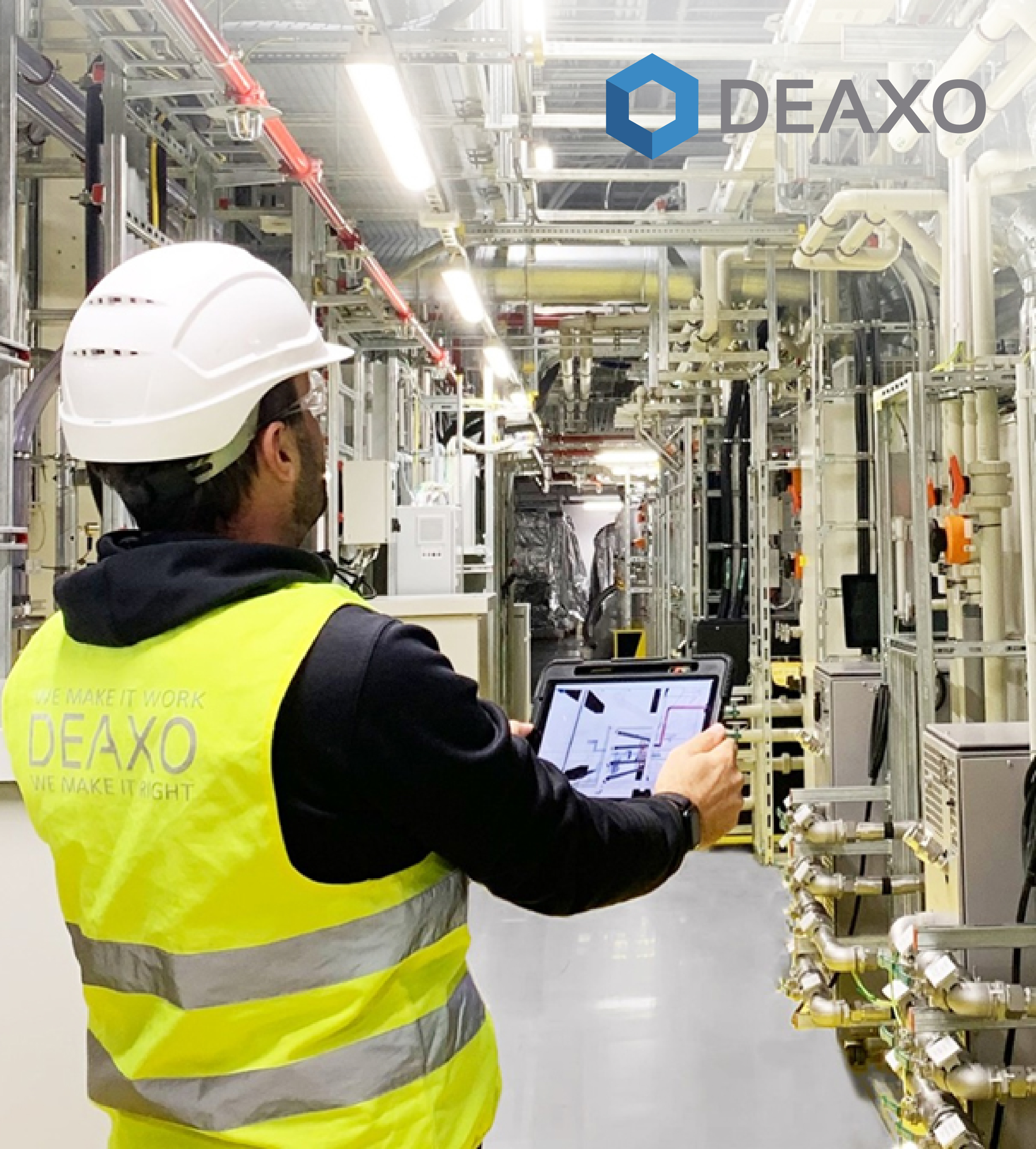
DEAXO is a trusted partner for complex Hook-Up projects in high-tech manufacturing environments. From planning and engineering to installation and production readiness, we providethe following services:
- Hook-up design (2D & 3D)
- Equipment cards
- Test & qualification
- Start-up and commissioning support
- Industrial engineering
- Space management
- Project management
- Site supervision during the installationphase
- QA/QC support
|
|
|
DEAXO is a trusted partner for the successful delivery of complex high-tech projects. Acting as an EPC, EPCM or PMC partner, we support our clients throughout the entire project lifecycle. We ensure transparency, control and reliable project execution.
By combining engineering expertise with structured project management and deep semiconductor industry knowledge, we help minimize risks, prevent delays and maintain alignment between technical, commercial and operational requirements.
Our services include:
- Support in execution of customers’ program to meet budget, schedule & quality
- Support during early project phases with required upfront planning & early works
- Creation of project execution plan
- Project scheduling
- Critical path analysis
- Risks management and control
- Design review / check-up
- Claim management
- Procurement support
- Site supervision
- Support and management with authorities
|
|
|
|
Dr. Schenk GmbH, established in 1985, is an innovative high-tech company based in Graefelfing near Munich, Germany. Dr. Schenk develops, produces and markets optical inspection and measurement solutions for automated quality assurance and production process monitoring. This includes high-quality customizable handling solutions. The systems are a key success factor in the making and converting of many materials, e.g. plastics, nonwovens, metal, paper, glass, or structured surfaces for a multitude of markets such as display glass, consumer electronics, automotive, packaging,medical, new energy, and many more.
Throughout the world Dr. Schenk’s 300+ employees continue to set new standards for inspection.Over 18,000 m² of modern, cleanroom-capable production and testing facilities are available to research,development and production to apply cutting-edge optics and electronics to customer applications.
Dr. Schenk offers extensive from -lab-to-fab knowledge. Customers benefit from the expertise in the translation of lab applications to large-scale productions. Sophisticated handling solutions completethe one-stop-shopping experience.
The company’s objective is complete customer satisfaction. This is achieved through innovative and practical solutions that can be implemented into new and existing production lines. Local sales and service facilities around the world ensure fast support, technical service, training and consulting at any phase of a project.
From modular standard units to highly customized systems – Dr. Schenk’s solutions have your material in focus!
|
|
|
Products / Service Introduction
|
|
Auto Optical Inspection System
|
|
|
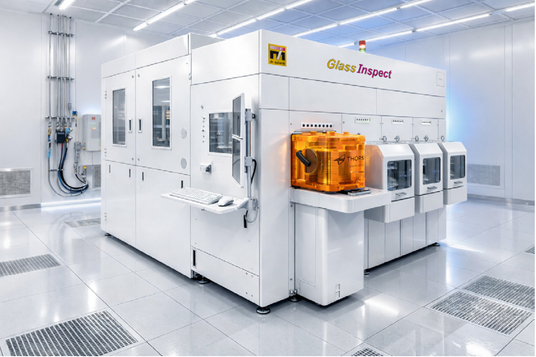
In the advanced packaging and pan-semiconductor industries, Dr. Schenk surface inspection solutions have become essential for many companies seeking to improve yield and ensure reliability. Particularly in advanced packaging processes such as FOPLP (Fan-Out Panel-Level Packaging), the company has set the industry standard by achieving high detection rates and accuracy for critical low-contrast defects—such as particles and micro-scratches—on glass substrates, leveraging its proprietary MIDA/MIDAX multi-angle defect analysis technology and next-generation AIMI intelligent inspection technology. In the field of TGV (Through-Glass Via) technology, Dr. Schenk, drawing on its extensive experience in glass substrate inspection and leading optical inspection technology, provides critical online and offline inspection solutions for TGV process parameters such as glass via quality, metallization fill effectiveness, and surface pattern accuracy, effectively supporting customers’ transition from laboratory R&D to large-scale mass production.
|
|
|
Economic Development Agency Brandenburg (WFBB)
|
|
|
Economic Development Agency Brandenburg (WFBB) is the central business development agency of the German state of Brandenburg. It supports investors, companies, startups and research institutions with site selection, investment projects,funding opportunities, innovation, skilled workforce recruitment and market entry.
Working closely with regional, national and international partners, WFBB helps businesses identify suitable locations,connect with relevant stakeholders, navigate public authorities and access public funding and research networks.
Brandenburg is home to globally competitive industries, including semiconductors and microelectronics, renewable energy,clean technologies, advanced manufacturing, mobility, life sciences and the circular economy. WFBB actively supports projects that strengthen these sectors and contribute to the transition towards a climate-neutral and innovation-driven economy.
As a publicly funded organization, WFBB provides confidential, impartial and generally free-of-charge advisory services. Its mission is to attract investment, foster innovation and create sustainable economic growth by helping companies establish,expand and succeed in Brandenburg.
|
|
|
Products / Service Introduction
|
|
Brandenburg – European Microelectronics Investment Hub
|
|
Brandenburg in Germany is one of Europe's most attractive locations for microelectronics companies. Situated at the heart of the German capital region surrounding Berlin, it offers excellent access to international markets, a highly skilled workforce, and a strong research and innovation ecosystem. Companies benefit from competitive operating costs, available industrial sites, reliable infrastructure, and tailored investment support. Brandenburg is home to leading semiconductor, photonics, and advanced manufacturing companies and is closely connected to renowned universities and research institutes. As part ofthe European Union, Brandenburg provides direct access to the world's largest single market and offers opportunities to participate in strategic European initiatives aimed at strengthening semiconductor production and supply chain resilience. |
|
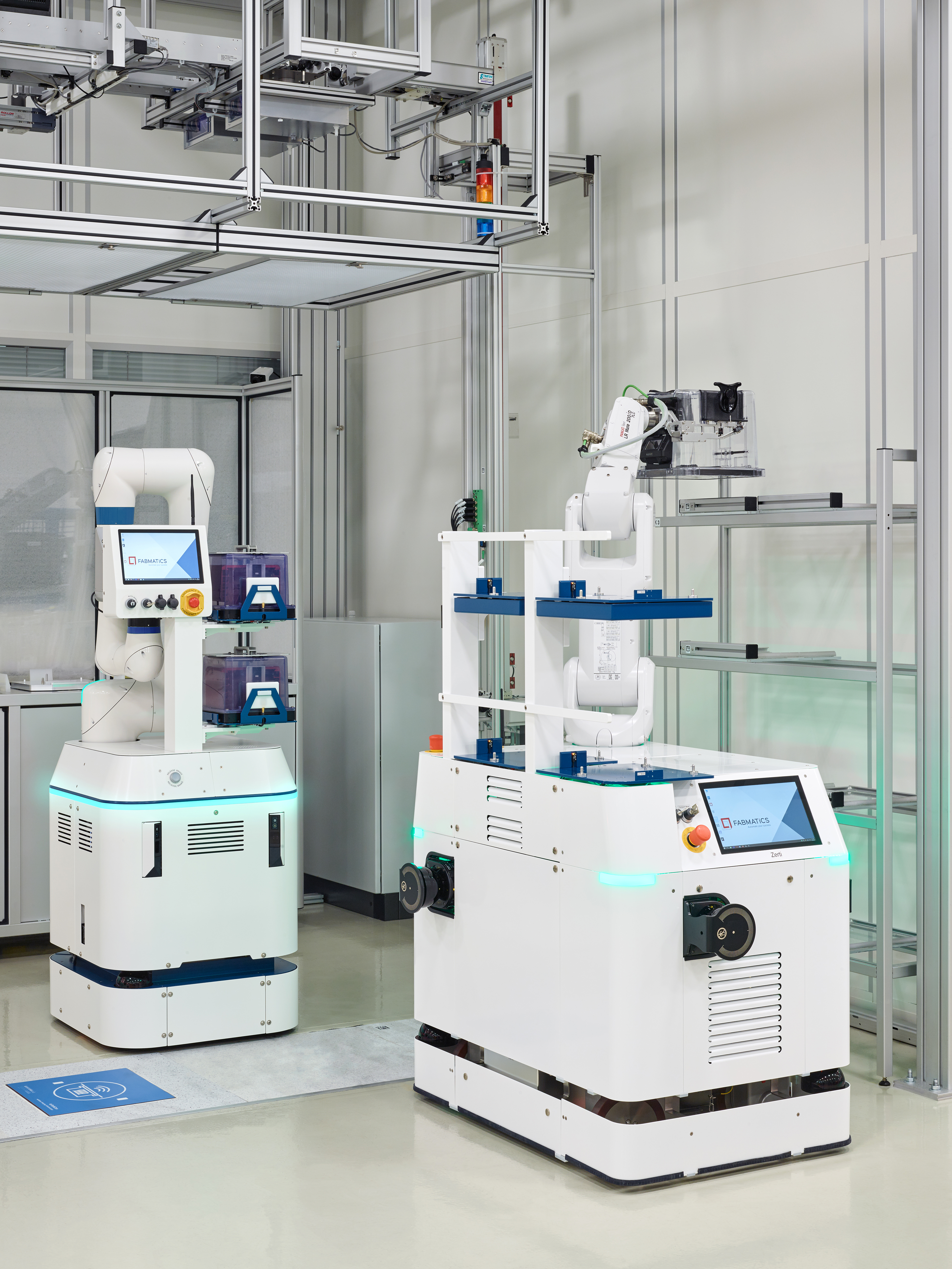
Fabmatics is a leading provider of automation solutions for semiconductor manufacturing, specializing in material handling, intralogistics, and factory integration. With over 35 years of experience, Fabmatics supports both greenfield and existing 200 mm and 300 mm fabs in optimizing efficiency, throughput,and reliability.
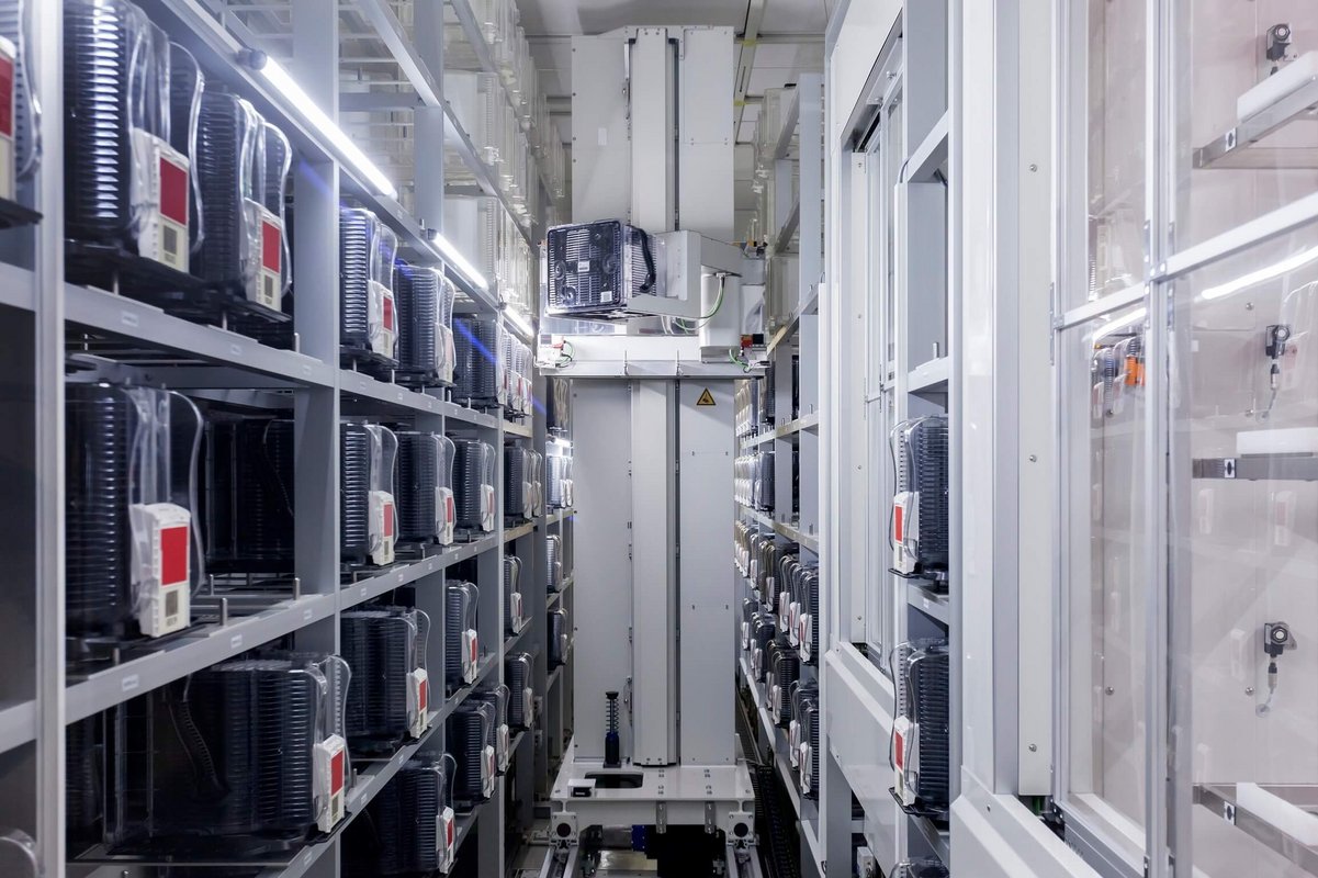
As a one-stop partner, Fabmatics offers a comprehensive portfolio including handling systems, transport solutions, mobile robots, software integration, identification technologies, purge systems, and intelligent storage solutions—such as advanced stocker systems designed for high-performance cleanroom environments.
With a strong global footprint across Europe, the US, and Asia, Fabmatics combines system integration expertise with deep application knowledge in semiconductor fabs.
In Taiwan, customers are supported locally through the long-standing partner GBG Technology Co.,Ltd., ensuring fast response times, on-site service, and close collaboration in one of the world’s most important semiconductor hubs.
Fabmatics stands for intelligent automation, strong partnerships, and measurable results—helping fabs transform complexity into performance.
|
|
|
Products / Service Introduction
|
|
Our stocker portfolio offers a comprehensive range of automated cleanroom storage solutions tailored to different fab layouts,capacity needs, and material types:
· Floor-based stockers
Linear Stocker, Max Stocker, RadialStocker, Cube Stocker – designed forhigh-density storage, flexible scalability, andreliable automated storage and retrieval.
· Ceiling-mounted systems:
Flat Stocker – enabling zero-footprint storage by utilizing overhead space and maximizing valuable cleanroom floor area.
· Supported product carriers:
FOUPs, FOSBs, SMIF pods, open cassettes, boxes, and reticle pods – ensuring compatibility across various fab processes
· Optional features:
Integrated purge functionality for contamination control and yield protection, as well as seamless integration into fab automation systems
|
|
|
Our mobile robot portfolio enables flexible,scalable, and cleanroom-compliant material transport and handling in semiconductor fabs,supporting both automation upgrades and new installations:
HERO Fab (200 mm / 300 mm):
High-throughput solution for wafer transport with direct tool integration – ideal for continuous front-end production and stable,high-volume operation
HERO Scout:
Flexible robot for reticle pods and sensitive materials, featuring high vertical reach for accessing elevated tools and stockers and optimized for areas with high human traffic
Common strengths:
High quality, reliability, and safety for both material and people, ensuring long-term performance in demanding fab environments
System control:
HERO LogIQ fleet manager for centralized coordination and optimized material flow
|
|
|
Our OEM Service Offering supports Taiwanese semiconductor equipment manufacturers in establishing and operating their business in Europe, with a strong focus on the Silicon Saxony region.
As a local partner, we provide comprehensive support across the entire equipment lifecycle:
· Installation & Integration:
Fast and seamless setup within existing fab environments
· On-site Service & Maintenance:
Preventive and corrective support to ensure maximum uptime
· Technical Support & Training:
Local expertise, operator training, and hands-on assistance
· Upgrade & Retrofit Services:
Adaptation of equipment to European standards and fab requirements
· Third-Party Service:
Acting on behalf of OEMs to strengthen local customer relationships
With decades of experience in semiconductor automation and a strong presence in Dresden, we bridge the gap between Asian OEMs and European fabs—reducing complexity, accelerating market entry, and ensuring reliable long-term operations.
|
|
|
|
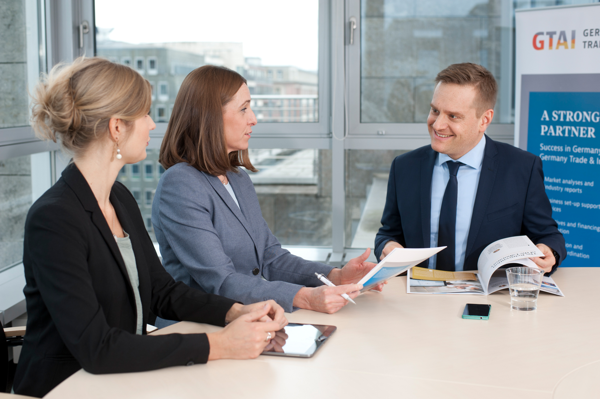
Germany Trade & Invest (GTAI) is the Federal Republic of Germany's international economic promotion agency. GTAI supports international companies expanding to and in Germany. GTAI experts offer free,confidential advice and project support for firms wishing to take full advantage of Europe’s largest market by establishing subsidiaries in Germany.
|
|
|
Products / Service Introduction
|
|
|
Our free-of-charge services for investors include:
- Consulting on individual market entry strategy
- Industry specific market data and statistics
- Information on the German tax and legal framework
- Information on finance and incentive options
- Active support in finding the best business location in Germany
|
|
|
|
Hoenle is a leading provider of UV technology and water treatment solutions for high-purity applications. With decades of experience in ultraviolet technology, we support semiconductor manufacturers worldwide with innovative systems for TOC reduction, UV oxidation, and ultrapure water treatment.
Our solutions are designed to meet the demanding requirements of the semiconductor industry,helping customers achieve the highest standards of water quality, process reliability, and production efficiency. From wafer fabrication to advanced chip manufacturing, Hoenle technologies contribute to stable processes and sustainable operations.
As part of a global group of companies, we combine engineering expertise, application knowledge, and local customer support to deliver customized solutions for semiconductor facilities around the world.At SEMICON Taiwan, we are pleased to present our latest UV technologies for ultrapure water applications and discuss how our solutions can help optimize your manufacturing processes.
Visit us to learn more about our innovative approaches to water treatment and semiconductor production, and discover how Hoenle can support your path toward greater efficiency, quality, and sustainability.
|
|
|
Products / Service Introduction
|
|
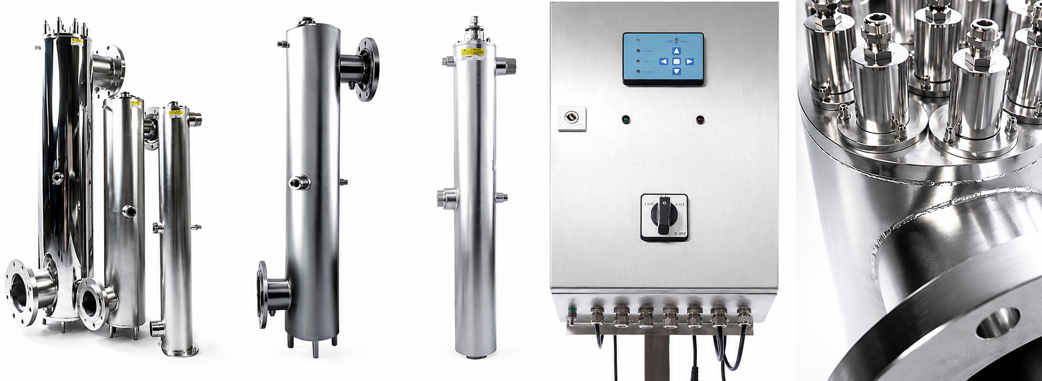
Hoenle TOC UV reactors are specifically designed for ultrapure water (UPW) applications in semiconductor manufacturing. Utilizing high-performance 185 nm UV technology, theyefficiently oxidize and reduce Total OrganicCarbon (TOC) to ultra-low levels, supporting the stringent water quality requirements of advanced semiconductor processes.
Engineered for reliable operation, optimized hydraulic performance, and maximum UV efficiency, our reactors ensure consistent water quality and stable production conditions. Available as customized solutions,Hoenle TOC reactors can be seamlessly integrated into new or existing UPW systems, helping manufacturers improve process reliability,product yield and operational efficiency.
|
|
|
|
The Chamber of Industry and Commerce (IHK) Aachen represents 85,000 businesses across the Aachen region, a strong hub for semiconductors and related technologies-such as equipment, R&D, materials and laser applications.
Located at the intersection of Germany, Belgium, and the Netherlands, the Aachen region sits within one of Europe's most dynamic semiconductor clusters. Within roughly 100 km, you'll find Leuven's world-leading chip research (imec), Eindhoven's semiconductor manufacturing champions (ASML, NXP), and Aachen's innovation powerhouses-the RWTH Aachen University and Forschungszentrum Jülich, as well as a strong industry cluster. This proximity creates unmatched opportunities for technology partnerships, supply chain integration, and market access across borders.
As a partner of this delegation, the IHK Aachen leverages its deep regional expertise in semiconductors and related technologies to connect you with innovative companies and key players-facilitating partnerships across borders.
|
|
|
intap – Your Strategic Relocation & Intercultural Partner in Germany
intap supports international companies in bringing talent to Germany smoothly, safely, and successfully. Based in Dresden, Saxony’s semiconductor hub, and with a branch office in Taiwan, we are a full-power, locally rooted team with a unique edge for companies hiring from Taiwan and Asia.
We do more than handle paperwork — we understand people, culture, and expectations. With Taiwanese expertise in-house, including one Taiwanese colleague based directly in Taiwan, we know what international talents need to feel truly welcome, secure, and at home in Germany.
Our team is physically on the ground in Dresden — no distant call centers, no one-person show. We personally guide employees through every step with our signature Saxon-Asian warmth: visas, registrations, driver’s licenses, housing, daily-life orientation, and integration.
Thanks to strong local authority contacts, we help fast-track bureaucratic processes. Through our premium housing network, we also access reliable landlords beyond the open market.
In addition, intap delivers hands-on intercultural training for leaders and employees worldwide, helping teams collaborate across cultures and ensuring a smooth transition into life and work in Germany.
Trusted by leading semiconductor players, intap helps international hires feel at home — faster.
|
|
|
intap provides a holistic relocation service for companies and international professionals moving to Germany. We support employees and their families from the very first step: visa and immigration processes, residence permits, document preparation, appointment coordination, and fast-track procedures with German authorities.
Once in Germany, we guide newcomers through all essential formalities, including city registration, bank accounts, health insurance, driver’s license exchange, vehicle registration, and everyday administrative tasks intap-network.de. Our service also covers housing search, lease review, handovers, utilities, kindergarten and school placement, doctors, orientation, and complete settling-in support.
With multilingual implementation — including Mandarin through our Taiwanese colleagues — we ensure a smooth, personal, and culturally sensitive arrival experience. When employees leave Germany, our departure services cover deregistration, contract management, and relocation logistics.
intap makes relocation simple, structured, and stress-free.
|
|
|
|
intap strengthens international teams with practical intercultural training for leaders and employees — especially for Taiwanese companies operating in Germany and organizations working with Taiwanese business partners.
Our tailored trainings help teams understand cultural expectations, communication
styles, decision-making processes, feedback culture, hierarchy, and collaboration patterns between Taiwan, Germany, and other international environments. The goal: fewer misunderstandings, faster alignment, smoother project execution, and more efficient teamwork.
We support onboarding, leadership development, international assignments, and the resolution of existing cultural challenges. New colleagues also benefit from orientation courses that make it easier to adapt to life and work in Germany.
Our certified trainers combine expertise in intercultural competence, organizational development, and leadership coaching. Trainings are available as half-day workshops, modular programs, or 1:1 sessions — onsite or digital, in German, English and mandarin.
With intap, international teams collaborate with more clarity, trust, and productivity.
|
|
|
|
Invest Region Leipzig (IRL) is the investment promotion agency for the Leipzig Region in Germany. We provide comprehensive support for investment and location decisions for your company's expansion. Our expert consulting team provides you with customized advice based on the specific site and business requirements for your growth. We support the site selection process and inform about the local labour market and recruitment, available grants and subsidies, facilitate access to relevant local networks and support with marketing activities. Your benefit is our continued support throughout the whole process of setting up a new site. We are here to enable your successful and smooth soft-landing in the Leipzig Region.
|
|
|
Products / Service Introduction
|
|
|
KPMG is one of the world’s leading audit and advisory firms, with extensive experience in managing international employee assignments. We offer integrated, tailor-made solutions that address all key legal aspects—including immigration, tax, employment law, and social security—from a single source.Our global network and deep industry knowledge enable us to support semiconductor companies inthe seamless and compliant relocation of employees to Germany. Visit us at the trade fair to discover how KPMG can be your trusted partner for international workforce mobility and business success.
|
|
|
Products / Service Introduction
|
|
Integrated Global Mobility Services from a Single Source
|
|
|
KPMG offers fully integrated global mobility services from asingle source, covering all key aspects of German-relatedassignments: immigration, tax, social security and employment law. Our services range from visa and work permit processes (including EU Blue Card) and registration requirements to tax and social security planning, payroll implications and HR/legal compliance.
Our multidisciplinary teams work closely together to design holistic solutions that align immigration, tax and HR considerations in a consistent way. This integrated approach reduces risks, avoids conflicting structures and creates transparent, efficient frameworks for both employers and employees.
For companies active in or connected to the semiconductor industry, we help build robust global mobility frameworks that enable compliant, cost-effective and business-driven deployment of key talent to Germany. We work in very close collaboration with our KPMG colleagues in Taiwan to ensure seamless support across both jurisdictions.
|
|
End-to-End Immigration & Work Permit Services for Germany
|
|
KPMG provides end-to-end immigration and work permit services for companies deploying staff to Germany. We support employers and employees throughout the entire process, from initial immigration strategy and choice of permit (including EU Blue Card) to the preparation of application documents, coordination with German authorities and follow-up after arrival.
Leveraging the experience gained from handling thousands of immigration cases per year, we offer efficient, reliable and practice-oriented solutions. Our services cover visa applications, residence and work permits, registration requirements, extension and change of status, as well as related compliance aspects (e.g. notification obligations and documentation). We work closely with HR and mobility teams to ensure a smooth, predictable and legally compliant process.
For companies active in or connected to the semiconductor industry, we help secure the right immigration solutions for highly qualified specialists, project staff and executives—enabling fast, compliant and business-driven access to talent in Germany. In addition, KPMG Law provides comprehensive German employment law advice to ensure that immigration solutions are fully aligned with contractual and HR requirements.
|
|
Tax & Social Security Advisory
|
|
|
KPMG advises employers and employees on the tax andsocial security implications of cross-border assignments involving Germany. Our services include tax planning, payrollsetup, withholding obligations, social security assessments,and compliance with German and international regulations.We help semiconductor companies design assignment structures that are tax-efficient and compliant, avoiding double taxation and unforeseen liabilities for both the company and its employees.
|
|
mechatronic systemtechnik GmbH
|
|
|
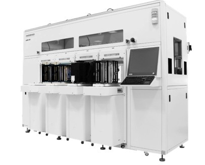
Fully automated and modular handling systems for complex handling requirements
mechatronic systemtechnik, is a leading global supplier to the semiconductor industry specialized on fully automated handling systems for non-standard substrates and handling requirements. These solutions are capable of handling multiple wafer types and sizes in a single platform and also address complex handling requirements at the highest levels of safety and reliability. mechatronic systemtechnik’s product portfolio includes fully automated wafer loader (EFEM) systems, wafer packer, wafer sorter, cutting & removing of TAIKO ring and calotte loader. A trusted partner with major wafer fabrication plants and semiconductor equipment suppliers mechatronic systemtechnik has created a worldwide network and strong global service support aimed to offer fastand reliable solutions.
|
|
|
Products / Service Introduction
|
|
|
Sorting, splitting and merging of all types of critical wafers and film frames
|
|
|
Wafer Packer / Unpacker (mPT)
|
|
|
Fully automated Packer/ Unpacker of wafers/ frames to/ from shipping boxes to/from cassettes or FOUPs
|
|
|
Ring Cutter and Remover (mRR & mLC)
|
|
|
A fully automated solution, cutting and removing of the ring are integrated into one process step improving productivity in combination with increased performance.
|
|
|
|
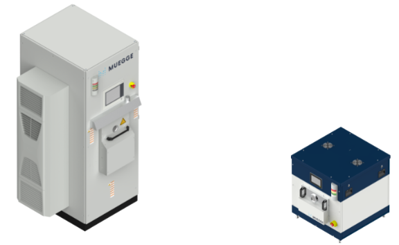
The MUEGGE Group is a globally positioned leader in microwave and plasma technology with 40 years ofexperience. Headquartered in Germany with locations in the USA, Italy, and Singapore, MUEGGE delivers advanced plasma sources, microwave generators incl. solid-state generators and critical process components for semiconductor applications, such as PECVD, PEALD, etching of organic and inorganic materials, chamber cleaning, resist removal and decapsulation.
Our portfolio includes microwave generators operating at 915 MHz and 2.45 GHz with power levels ranging from 1 kW to 100 kW, as well as waveguides, matching components, magnetrons, highly reliable solid-stategenerators and advanced plasma solutions. These include plasma arrays for large-area deposition, remote plasma sources (RPS), atmospheric plasma sources, downstream plasma sources and decapsulation and stripping tools.
Beyond semiconductor manufacturing, MUEGGE provides tailored microwave and plasma solutions for awide range of industries, including lab-grown diamonds, hydrogen production, power-to-X, photovoltaics,industrial drying, food heating and medical applications.
With a global footprint, strong engineering expertise and a commitment to innovation, quality andreliability, MUEGGE helps customers worldwide overcome complex process challenges and achieve outstanding performance across diverse high-tech industries.
|
|
|
Products / Service Introduction
|
|
Designed for damage-free, high-throughput semiconductor processes
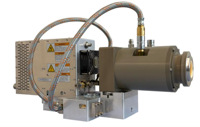
The MUEGGE Remote Plasma Source operates from 300 W to 3 kW at process pressures between 0.27 and 7 mbar, enabling high-density plasma generation under industrial conditions. The applicator generates a high flux of neutral reactive radicals (O, N, H, F-based species) while effectively suppressing ion energy. This maximizes chemical reactivity without physical surface damage and ensures reproducible process stability.
Features
- Pure chemical and isotropic etching
- No ion bombardment
- Low thermal load on the substrate
- No electric field and plasma in the process chamber
- No charging of the substrate
- High electron/radical densities
Suitable for the following Semiconductor Applications:
Isotropic wafer and chamber cleaning for complex 3D geometries, high-selectivity resist and polymer removal, SU-8 and LIGA processing, Atomic Layer Deposition and Etching (ALD/ALE), surface activation and damage-free decapsulation processes.
|
|
|
Fast, selective and damage-free decapsulation of microchip packages.
The extremely gentle process conditionsensure outstanding materialcompatibility. Critical metals such ascopper, gold, aluminum, and Cu/Pd alloysremain unaffected, making thetechnology ideal for delicate structureslike wire bonds. Chip passivation layersare only minimally attacked, withselectivity values exceeding 500:1.
- Fast, isotropic etching by radical
- Simultaneous decapsulation of microchips
- No ions, no microwave radiation, no electrical fields in the area of the samples
- Very low thermal impact only by chemical reaction energy due to the effect of the radicals
- Very high removal efficiency (>200μm/h) including inorganic filler materals
- No attack on bonding wires made of e.g. Au, Al, Cu, Cu/Pd · Only slight etching of chip passivation (high selectivity > 500:1)
- Short decapsulation times: typically 1 - 3 hours after laser ablation
- Efficient removal of packaging and mold/epoxy in particular
- Die surface is preserved
|
|
|
|
Rauschert was founded in 1898 and has been focusing on the manufacture of ceramic precision components and providing wastewater filtration systems and engineering solutions for a century.
The applications have been expanding to textiles, metal processing, medical, household, energy and water treatment technology. Filtration wise, providing 100% German-made MF, UF and NF ceramic membranes and automated filtration systems, flexibly responding to various process applications and customer needs, creating ESG value with energy saving and carbon reduction.
|
|
|
Products / Service Introduction
|
|
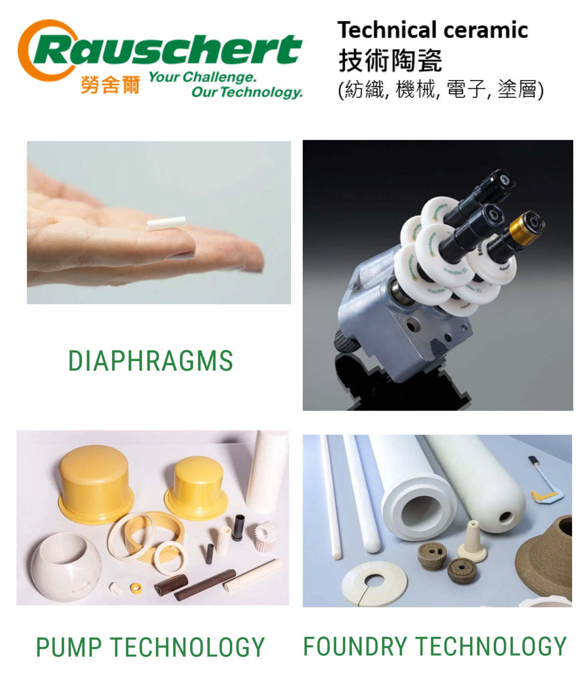
Our technical ceramic components offer outstanding hardness, long service life, and high resistance to heat and aggressive chemicals. By combining ceramics with metal or plastic in hybrid designs, we deliver lightweight, high-performance solutions tailored to various industries.
With expertise in material selection, surface treatment, and precision manufacturing, we provide custom components for applications in household appliances, laboratory and heating systems, textile machinery, shipbuilding, and infrastructure.Our product range includes :
- Ceramic heaters
- Mgo tubes
- Wire drawing components
- Coatings
- Pump and valve parts
- Textile ceramics (such as wire guides, godets, friction discs, and nozzles)
- Ceramic Diaphragm for pH sens
|
|
|
|
Ceramic filtration membrane/system
|
|
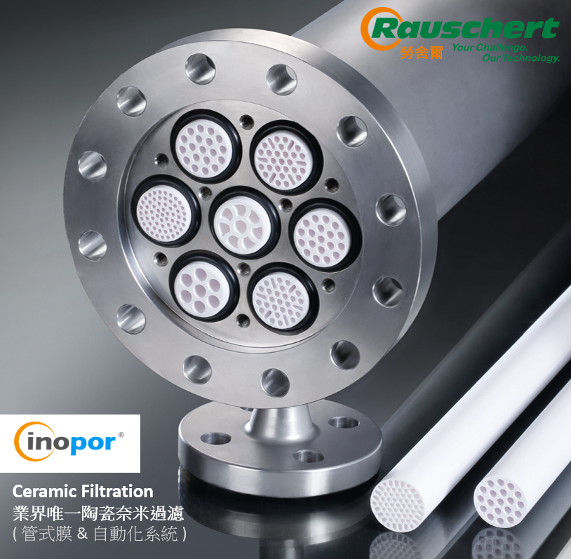
Our Inopor® ceramic filtration membranes deliver advanced micro-, ultra‑, and nanofiltration performance with outstanding thermal, chemical, and mechanical stability. Made from alumina, titania, zirconia or silica, they enable purely physical separation without chemical additives.
Available in tubular single‑ or multi‑channel modules from 100 mm to 1,200 mm long, and offering cut‑offs down to 200Da, pore size under 1nm. Inopor® is the only global supplier of ceramic nanofiltration membranes at this level. With growth of applications ranging from wastewater and process-stream separation to pharmaceutical and food/drink clarification, Inopor® supports robust, sustainable filtration to reach ESG target- even under extreme pH, temperature, and abrasive media.
|
|
|
Rheinisches Revier – NRW.Global Business
|
|
|
Rheinisches Revier – a hub for the future of industry: Be Part of It.
As Europe’s largest lignite mining region phases out lignite, Europe’s first climate-neutral industrialregion is taking shape! In North Rhine-Westphalia’s Rheinisches Revier, an extraordinary transformation is underway, supported by €14.8B in government funding. Open-cast mining is being replaced by key sectors such as Green Energy Technologies, New Mobility, Digital Technologies, and Life Science. Companies from around the world are invited to establish themselves in the region.
This transformation is backed by NRW.Global Business, which promotes Rheinisches Revier internationally and assists companies with relocation. The state’s foreign trade promotion agency also profiles and markets a wide range of commercial sites for both brownfield and greenfield projects.
Investors benefit from a location in the heart of Europe, energy security, and engagement with industry leaders. The region’s robust research landscape offers cutting-edge innovations and skilled specialists.Recent investments from Quanta Computer and Microsoft highlight Rheinisches Revier’s appeal, with Quanta focusing on automotive technologies and Microsoft developing AI centers. Rheinisches Revier is set to become Europe’s most exciting investment region. Be Part of It.
|
|
|
Products / Service Introduction
|
|
Site selection and support for business settlement in Rheinisches Revier
|
|
Saxony Trade & Invest Corp.
|
|
|
Saxony Trade & Invest (Wirtschaftsförderung Sachsen GmbH) promotes the business location Saxony, assists companies on investment projects and supports Saxony based companies in developing new markets and cooperative partnerships.
|
|
|
Products / Service Introduction
|
|
|
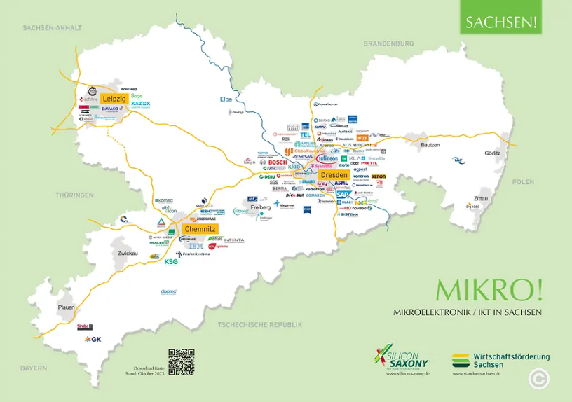
Information about the German federal state of Saxony,especially its microelectronics industry. Saxony Trade & Invest supports foreign companies in their set-up in Saxony with help in location, partner and funding search. As a governmental owned organization, our services are free of charge.
|
|
|
Overview Map Selected companies from the ICT /microelectronics sector in Saxony and regional focus areas
|
|
|
|
|
Silicon & quartz for semiconductor industry
SICO was founded in 1981 in Austria/Europe and specializes in the production of high-purity silicon and quartz glass for the semiconductor industry.
As an ISO 9001:2015 certified company, SICO manufactures complete furnace parts for various OEM furnacebrands. We are experts in producing high-purity silicon carriers, injectors, liners, tubes etc. for e.g.front-end LPCVD & high-temperature processes, as well as in the refurbishment, cleaning, and repair of components for the semiconductor industry. That with high-precision manufacturing, strong R&D expertise and patented silicon parts bonding technology. The SICO Global Group is represented in the USA, Europe,and Asia.
|
|
|
Products / Service Introduction
|
|
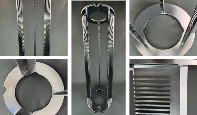
Silicon Wafer Carrier / Boat
|
|
|
As semiconductor manufacturing moves deeper into advanced LPCVD, diffusion, and high-temperature processes, fabs are becoming increasingly sensitive to critical challenges particle generation and thermal stress,slip lines, backside defects, or particles. This is where high-purity silicon carriers come into the game, as it minimizes thermally induced stress to the wafer at high temperatures, while improving process stability in LPCVD applications.
|
|
|
|
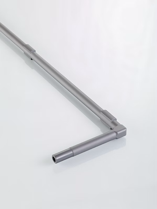
In LPCVD environments, even small differences in thermal expansion behavior between process hardware and deposited layers can generate particle defects over time.SICO’s silicon injectors are designed to mitigate these effects through a combination of ultra-high material purity,advanced surface engineering, patented injector geometries, and proprietary bonding technologies. That leads to fewer maintenance cycles, longer deposition runs,reduced downtime and improved tool utilization.
|
|
|
Refurbishing of EPI Quartz Parts
|
|
|
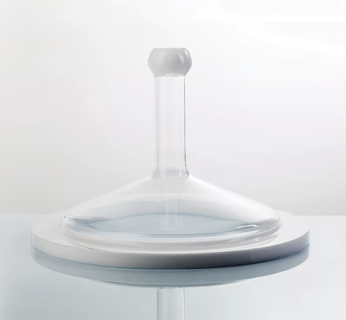
As a qualified OEM supplier SICO offers a state of the art ONE STOP SOLUTION for Epitaxial Growth (EPI), to improve tool uptime and reduce the cost of ownership. SICO takes care of the complete cleaning & repair process of your quartz parts at the new state of the art climatized hot work department in SINGAPORE, done by our senior master glassblowers. SICO helps to improve your parts with improved repair & refurb process steps to increase your tool uptime. SICO offers besides our premium Refurb & Repair-Servicefor all OEM´s, also new parts according to OEM specifications and additionally provides expertise to your customized modification needs.
|
|
|
|
Silicon Europe is the leading European alliance of clusters in (micro)electronics and digital technologies, fostering transnational collaboration to drive innovation, competitiveness, and European technological sovereignty.
As a globally recognized meta-cluster, we connect the major regional ecosystems in semiconductors, photonics,cybersecurity, AI, quantum, and emerging technologies, enabling a green and resilient economy.
We serve as the trusted voice of SMEs and start-ups, ensuring their representation in shaping Europe's economic security and industrial future.
|
|
|
Products / Service Introduction
|
|
Access to Europe’s Leading High-Tech Clusters
|
|
|
Silicon Europe Alliance serves as a single-entry point to 14 leading high-tech clusters across 9 European countries representing more than 2,500 organizations. Our membersare long-established innovation ecosystems at the forefront of semiconductors, photonics, cybersecurity, artificial intelligence, quantum technologies and other emerging technologies that drive Europe’s green, digital and resilient transformation. Through one trusted network, international companies, investors, research organizations and public institutions gain direct access to regional expertise,technology leaders, SMEs, research centers and innovation communities across Europe. The Alliance simplifies engagement with multiple European ecosystems, helping organizations identify the right region, partners and opportunities for collaboration, investment, technology sourcing and market access. By combining local expertise with European reach, Silicon Europe provides an efficient gateway to some of Europe’s most dynamic high-tech ecosystems.
|
|
Organization of Open Innovation Days
|
|
|
Turn your innovation challenges into tangible business opportunities. Silicon Europe Open Innovation Days connect corporates with innovative European SMEs,scale-ups and research organizations through a structured challenge-based scouting process. Based on your specific technology or business challenge, we launch and promote a European-wide call while managing the complete process, including communication, application handling, evaluation support and event organization. Companies can define different selection stages and decide which candidates advance throughout the process. Finalists are invited to pitch their solutions at a dedicated event hosted by one of our partner clusters in Europe, enabling direct exchange, matchmaking and collaboration opportunities NDA-based processes can be implemented where confidentiality is required. Following the event, Silicon Europe supports follow-up activities and provides success analysis to maximize long-term impact and partnership outcomes.
|
|
European Project Partner Matching
|
|
|
Access a trusted network of Europe’s leading high-techecosystems to identify the right partners for your international innovation and R&D projects. Through SiliconEurope Alliance, we connect organizations with innovative SMEs, research institutions and technology providers from 14 established clusters across 9 European countries. Our network includes more than 2,500 high-tech companies and research partners active in fields such as semiconductors, photonics, AI, cybersecurity, quantum technologies andadvanced manufacturing. Whether you are building a project consortium, preparing a funding proposal, expanding your innovation network or seeking specialized technical expertise, we help identify and engage the most suitable partners. Leveraging deep regional knowledge and stronglocal connections, Silicon Europe streamlines partner searchand collaboration across Europe, reducing time and effortwhile increasing the chances of successful cross-border innovation projects.
|
|
Thin-Film Deposition Equipment for Semiconductor Manufacturing
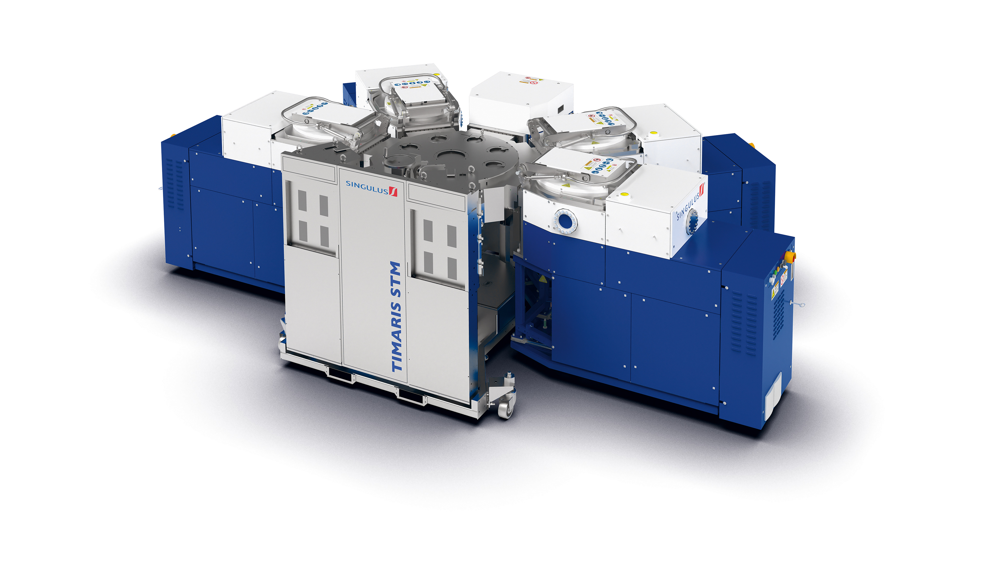
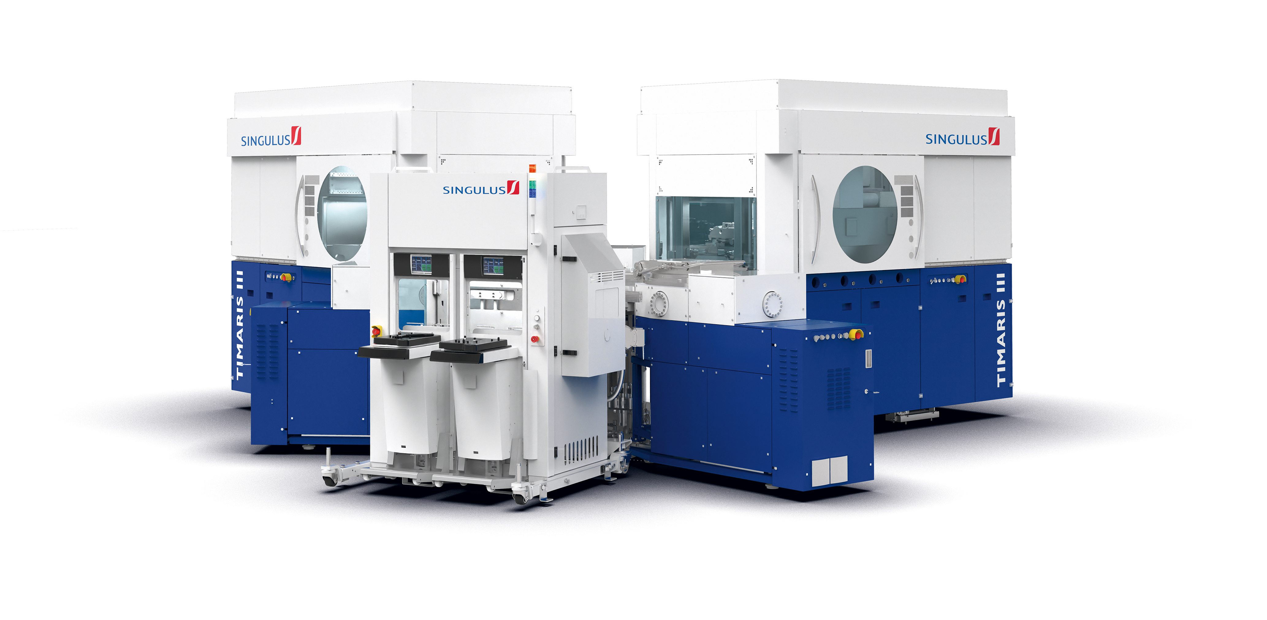
SINGULUS TECHNOLOGIES is a leading supplier of advanced thin-film deposition equipment for semiconductor and magnetics applications. Its solutions support the production of magnetic sensors(TMR, GMR, AMR), MRAM, integrated inductors, µLEDs, advanced packaging (RDL/UBM), interconnects,and other high-performance semiconductor devices.
The TIMARIS cluster platform combines multiple process modules with multi-target sputtering,integrated substrate heating and cooling, precise alignment, and an Applied Magnetic Field (AMF) option. This highly flexible configuration enables the deposition of complex multilayer stacks within a single process module, minimizing wafer transfers, reducing cleanroom footprint, and increasing throughput while ensuring outstanding process stability and film quality.
- Magnetic sensor (TMR, GMR, AMR,)
- Integrated inductors
- µLED
- Advanced Packaging (RDL, UBM)
- Integrated voltage regulator (Buck Converter)
- MEMS
- TMR, pTMR – MRAM
- High moment materials
- TFH reader & writer
|
|
|
Products / Service Introduction
|
|
The TIMARIS cluster tool is dedicated for the deposition (PVD sputtering/PECVD) of ultra-thin metallic and insulating films down to a thickness of one nanometer and below and stacks of such films with very precise material thickness and high uniformity specifications.
- 200 & 300 mm
- Metallization
- Reactive processes
- Dielectric films
- Interconnection
- Low damage ITO Micro-LED
|
|
|
The TIMARIS cluster tool is dedicated for the deposition (PVD sputtering/PECVD) of ultra-thin metallicand insulating films down to a thickness of one nanometer and belowand stacks of such films with very precise material thickness and high uniformity specifications.
· 200 & 300 mm
· Integrated voltage regulator
· High performance magnetic inductors
· Laminated layers with total thickness up to 8 μm
|
|
|
|
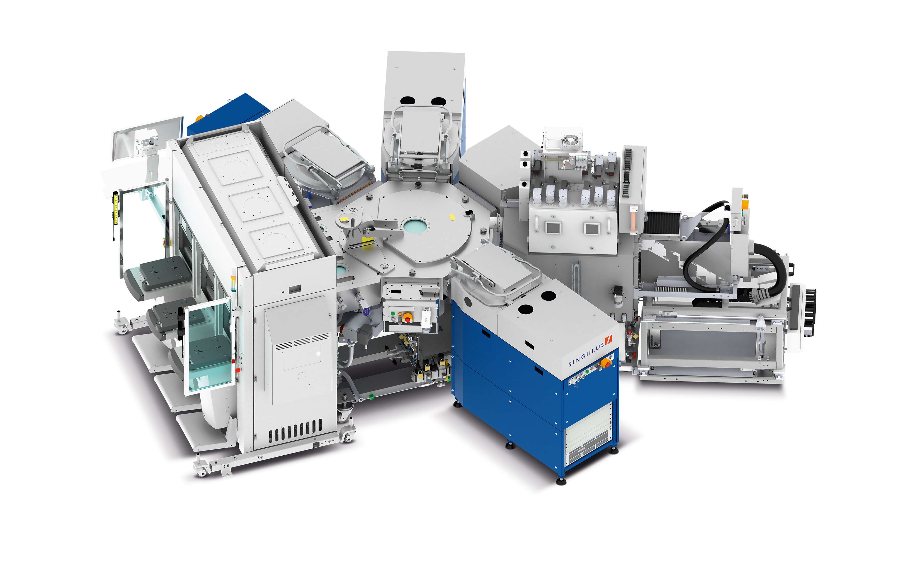
TIMARIS Production Platform
|
|
The TIMARIS cluster tool is dedicated for the deposition (PVD sputtering/PECVD) ofultra-thin metallic and insulating films down to a thickness of one nanometer and belowand stacks of such films with very precise material thickness and high uniformity specifications.
- 200 & 300 mm
- Emerging memory, e.g. MRAM, RRAM,PCRAM, etc.
- Magnetic sensors AMR / GMR / TMR· Advanced multilayers with very accurate thickness control
- Spintronics
|
|
|
|
SONOTEC is specialized in ultrasonic sensor technology in the field of non-contact and non-invasive liquid flow measurement and air bubble detection in flexible tubes and hard plastic pipes.
As a global technology leader, we offer excellent product quality, first-class measurement performance, and outstanding service to our customers in medical technology, biotechnology, and the semiconductor industry. In order to guarantee highest product quality, we are certified according to ISO 9001 as well as EN ISO 13485 and fulfil the directives for the manufacturing of products to be applied in potentially explosive atmospheres according to ATEX/IECEx.
In addition to our off-the-shelf products, we offer customized sensor solutions responding to application-specific requirements.
|
|
|
Products / Service Introduction
|
|
Ultrasonic Clamp-On Flow Meter SEMIFLOW© CO.65
|
|
|
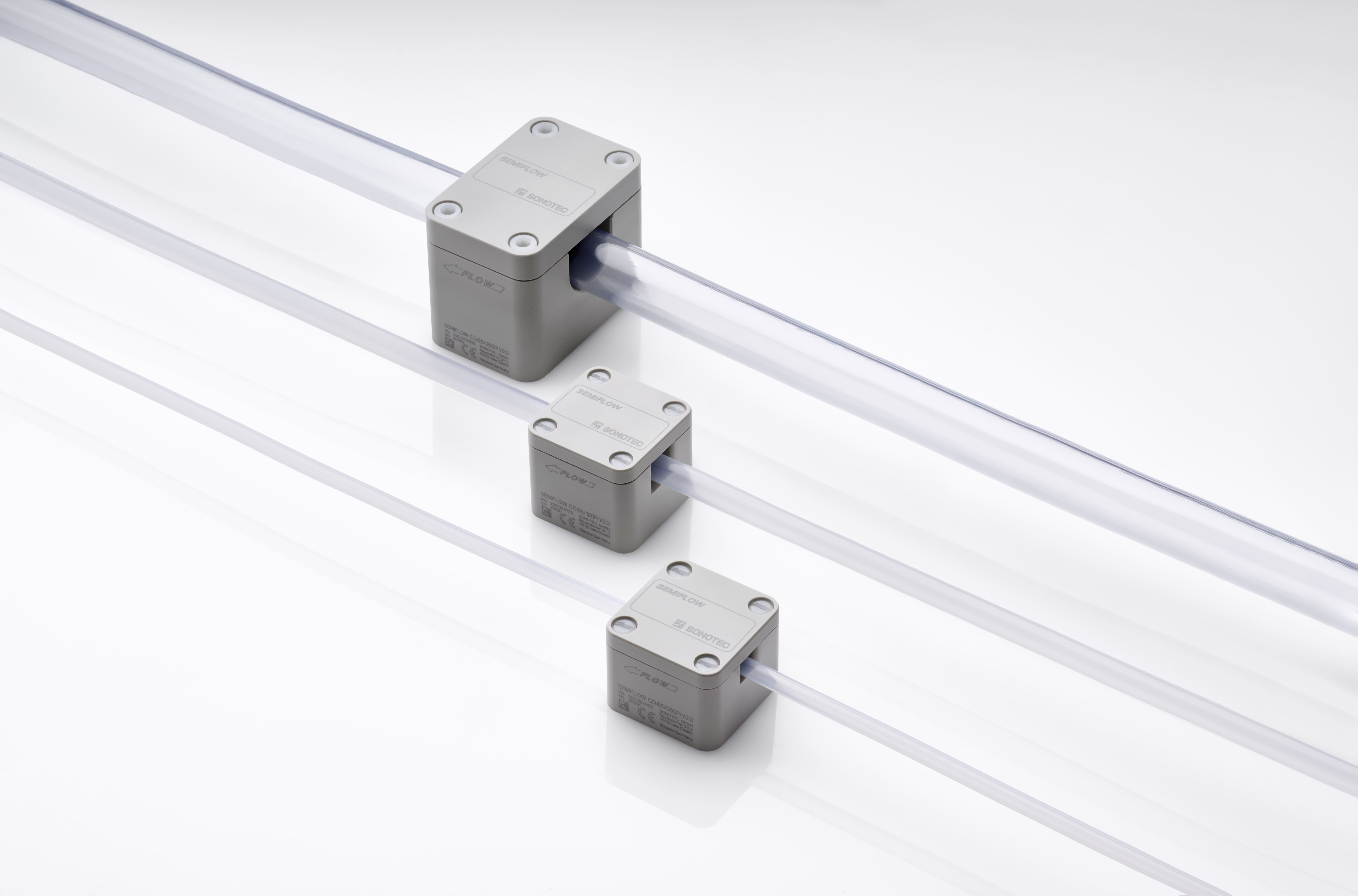
SEMIFLOW CO.65 clamp-on flow meters are specifically designed for the semiconductor industry. The highly precise and robust ultrasonic sensors measure directly through the rigid plastic tube or pipe without contact to the liquid,eliminating risks of leakages and contaminations, thus increasing uptime and maximizing yield. Their compact housing with integrated electronics board is perfectly suited for a convenient system implementation.
|
|
|
Ultrasonic Clamp-On Flow Sensor SEMIFLOW© CO.66
|
|
|
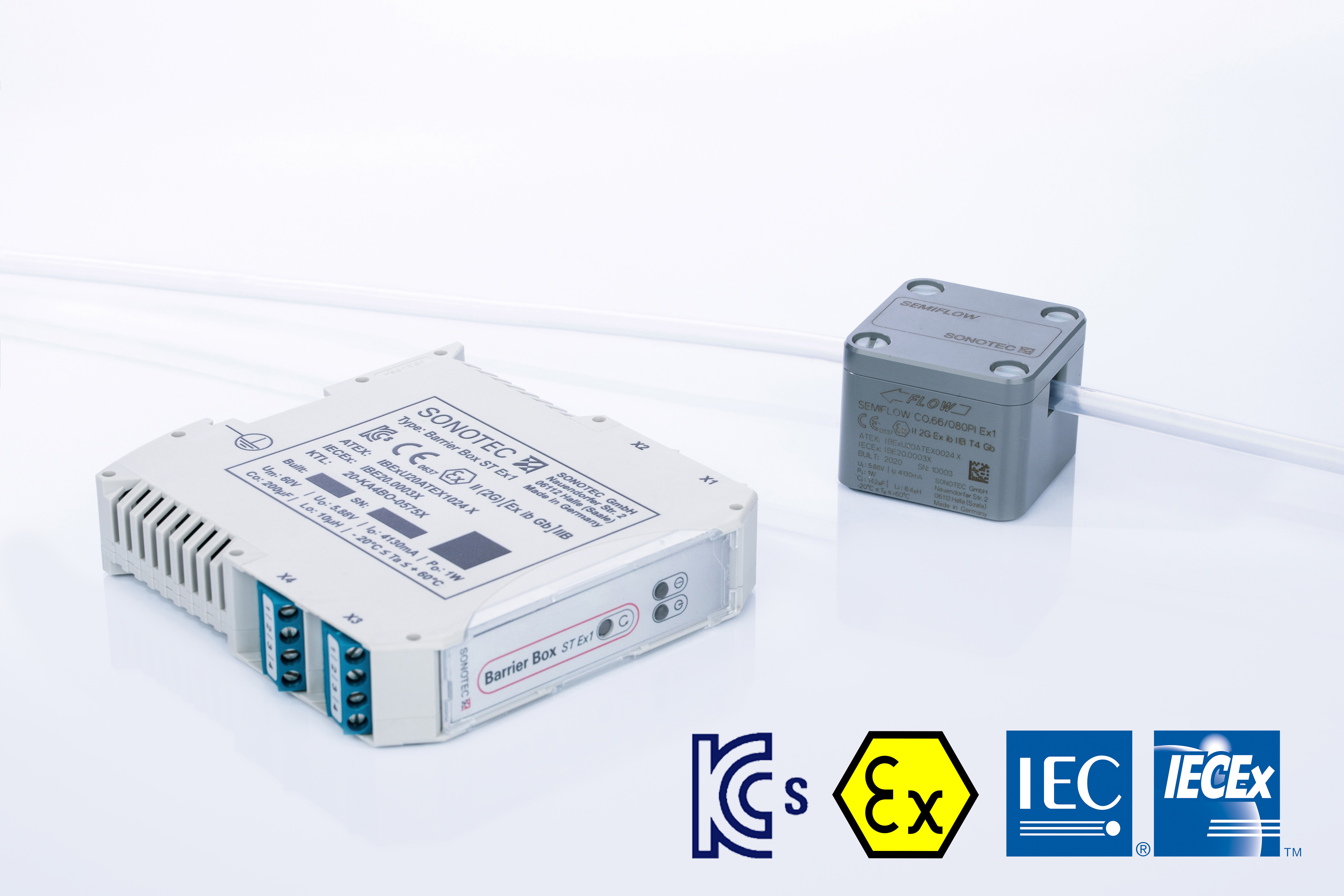
Specifically developed for the use in hazardous environments, the SEMIFLOW Ex1 Set opens a new product category for non-contact liquid flow measurement on rigid plastic tubing. It consists of the intrinsically safe SEMIFLOWCO.66 PI Ex1 flow sensor and the control gear Barrier Box ST Ex1.
|
|
|
Ultrasonic Clamp-On Bubble Sensor SONOCHECK© ABD06
|
|
|
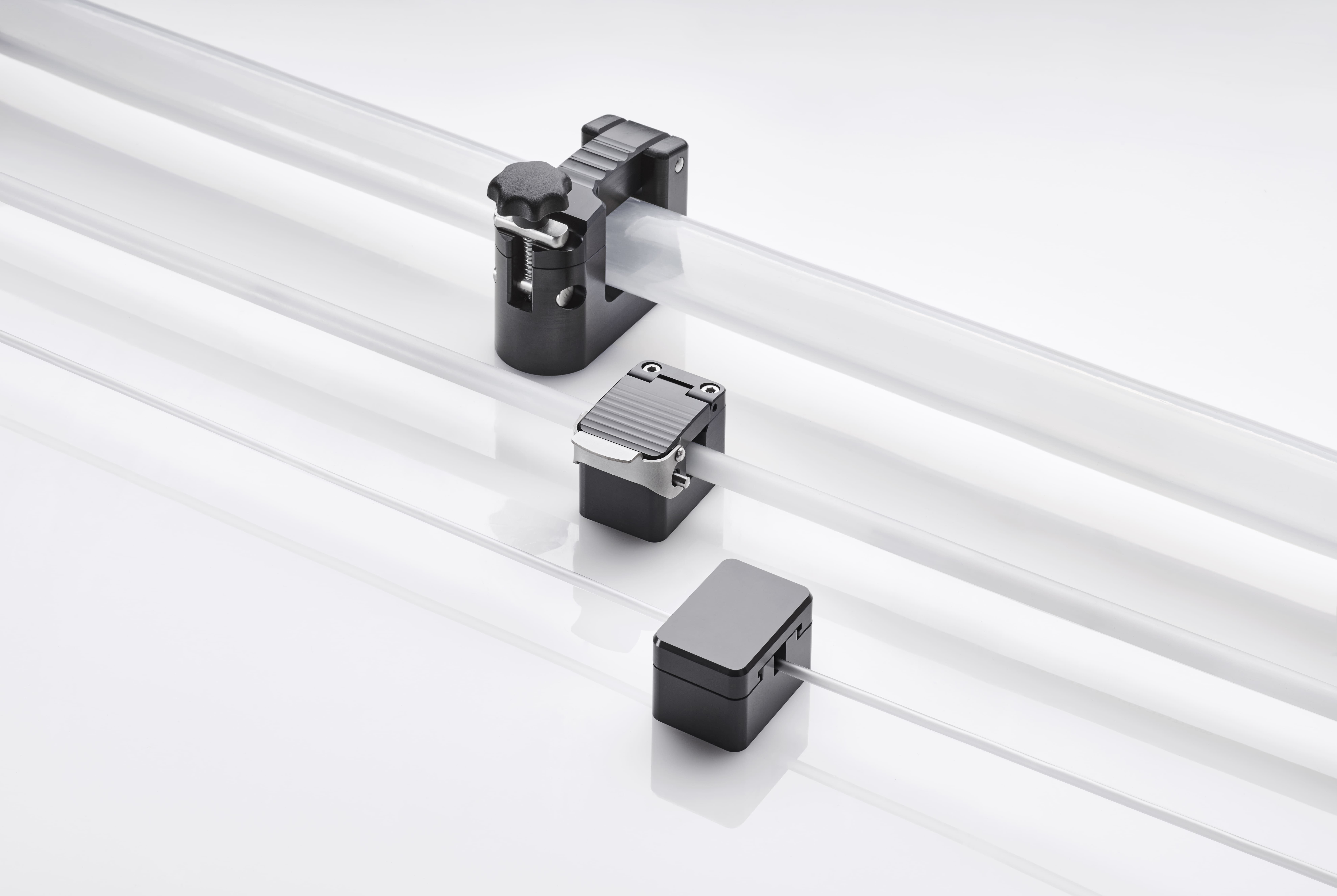
The non-contact air bubble detectors SONOCHECK ABD06 can spot bubbles as small as 1 μl and can also be used as full/ empty detectors. In critical processes of wafer manufacturing the presence of air bubbles or empty tube can lead to extensive consequences. Thus, their timely detection is crucial to save resources and increase production efficiency.
|
|
|
|
VACOM – Precision Vacuum Solutions for Modern Applications
For over 30 years, VACOM has delivered practical vacuum solutions that meet the needs of modern applications – from semiconductor manufacturing to cutting-edge research and analytical technology.
Our key strengths at a glance:
- Wide product range: Standard components, optical fibers, electrical feedthroughs, and advanced measurement technology.
- Application-focused sensors: NOVION for residual gas analysis and CASSINI vacuum sensors enhance system performance.
- Custom solutions: Tailored to meet specific customer requirements.
- Product configurator: Configure individual solutions in minutes with over 1,000 combinations.
- Industrial component cleaning: High-quality, reliable service.
Globally present, locally competent: With locations in Germany, Belgium, and the United States, VACOM supports customers worldwide as a trusted technology partner.VACOM combines precision, experience, and innovation to deliver reliable solutions that meet today's and tomorrow's technical challenges
|
|
|
Products / Service Introduction
|
|
|
The world of semiconductors is always evolving. Meeting emerging requirements demands customer-oriented,flexible and new solutions.
A deposition solutions specialist, VON ARDENNE offers comprehensive services to support our customers. Our high-precision engineering and materials science expertise enable custom design, engineering, manufacturing,commissioning and service for deposition equipment and components.
Our strong legacy in vacuum technology and deposition solutions, as well as materials and optics technologies,mean we excel in developing leading-edge semiconductor processes and equipment to meet each customer’s unique requirements.
|
|
|
Products / Service Introduction
|
|
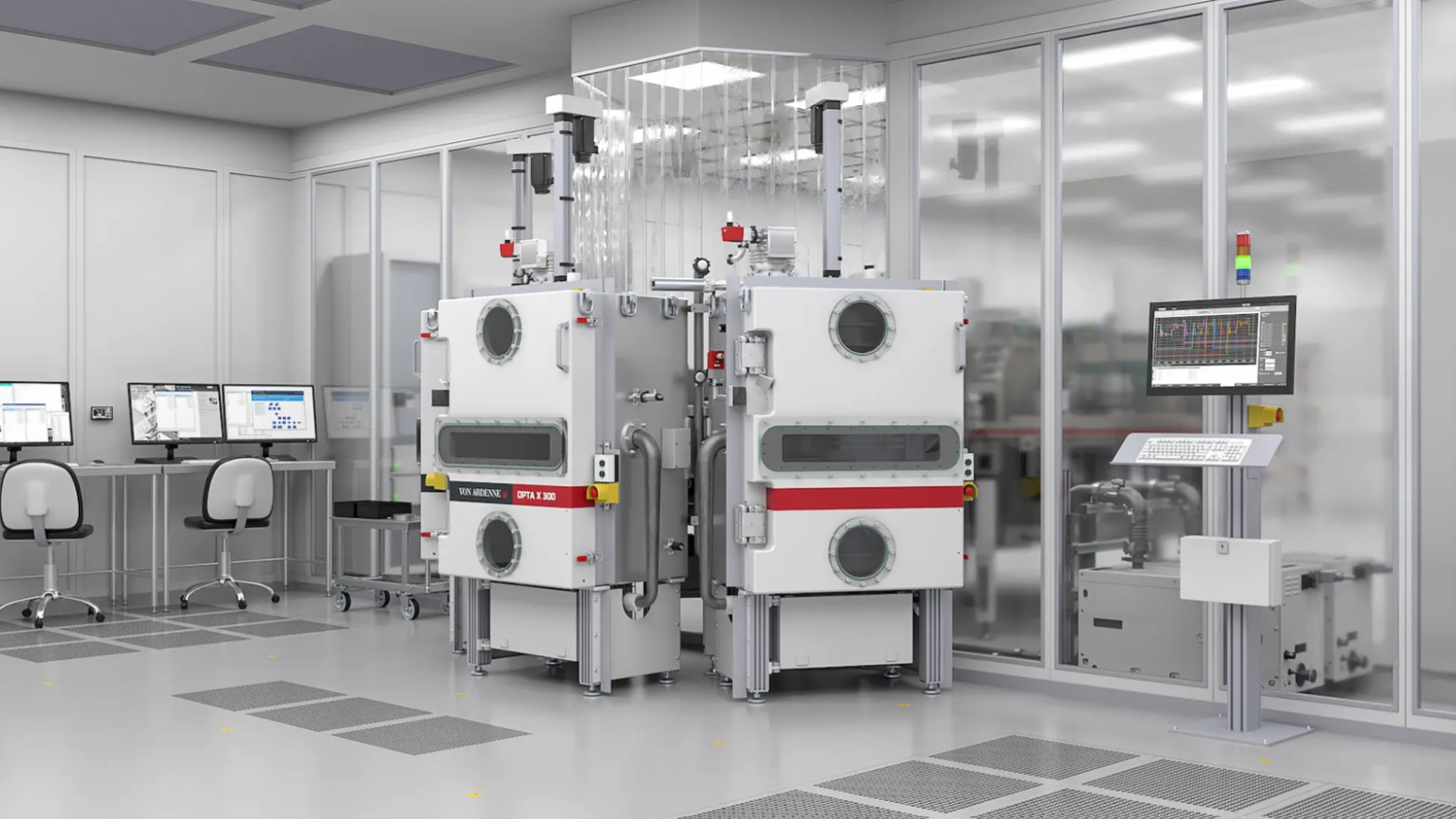
With the OPTA X200 and OPTA X300, we offer you highly productive coating systems. They are suited both for the most demanding optical coating systems and for the precise deposition of, for example, high-performance piezoelectric materials such as AlN and AlScN. This applies especially to multilayer optics with a high number of alternating layers and high-quality layer stacks for microelectronic applications and semiconductor systems.
The rotary disc systems coat both sides horizontally and are designed, depending on the model, for processing substrates with diameters of 200 mm or300 mm (including G12 wafers). For optimal coating, the special CARS technology is used. But other process modes such as Meta Mode, reactive or non-reactive sputtering are also available.
Both models are equipped with an automatic handling system. This is modularly constructed and enables safe loading with different substrates,which are guided through the system in adaptable carriers.
|
|
|
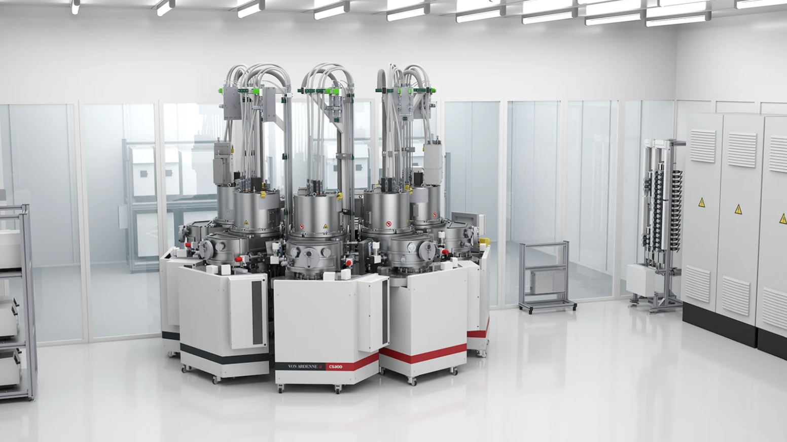
The cluster systems CS200 and CS300 are modular coating systems suitable for both highly flexible or highly productive processes in the development and production of applications in semiconductors,optics, and photovoltaics. They are specifically designed for processing substrates with a diameter of 200 mm or 300 mm (including G12 wafers).
Thus, our cluster systems are the ideal choice for the development of new coating technologies and the production of layers with specific properties and high reproducibility. Applications include sensors and through-silicon vias (TSV) for 3D advanced packaging technology in the semiconductor industry. Furthermore, the CS300 is used in the development of new solar cell generations such as TOPCon and perovskite tandem.
Thanks to their great flexibility, the cluster systems help reduce your operating costs.
|
|
|
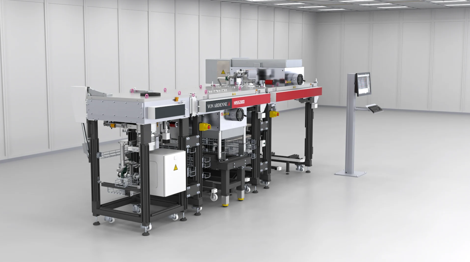
The HISS300 and HISS600 are modular coating systems designed for the horizontal coating of substrates. They are the ideal choice if you need a highly flexible production system with small to medium throughput, equipped with proven technology.
Thanks to their modular design, these systems can be configured to meet your specific needs. Various configurations are available, including a version with only one end, tailored for smaller production scopes.
The systems offer high process flexibility, supporting both sputtering and evaporation processes, as well as various pre- and post-treatment methods.
The flexible and dynamic design of the systems with standardized modules allows for customer-specific configuration. This adaptability enables customers to easily incorporate new processes or meet changing requirements, ensuring they can remain agile and responsive to product evolution.
|
|
|
|
GTO German Business Alliance
|
|
|
If you don´t want to receive any more messages (to: unknown@noemail.com) any longer, you can unsubscribe free of charge at any time.
Deutsches Wirtschaftsbüro Taipei
19F-9 No. 333 Keelung Rd
110208 Taipei, Taiwan
+886 2 87585800
info@taiwan.ahk.de
www.taiwan.ahk.de
|